Oblique hole etching method

An oblique hole and etching gas technology, applied in the field of microelectronics, can solve the problems of serious isotropic etching, loss of line width at the top of the inclined hole, long gas residence time, etc. loss, the effect of sidewall smoothing

Active Publication Date: 2017-10-13
BEIJING NAURA MICROELECTRONICS EQUIP CO LTD
View PDF6 Cites 0 Cited by
  • Summary
  • Abstract
  • Description
  • Claims
  • Application Information

AI Technical Summary

Problems solved by technology

[0004] First, the inclination angle of the oblique hole obtained by using the existing oblique hole etching method is about 60°, which cannot meet the requirements of certain processes. For example, in the field of 3D-IC, the inclination angle of the oblique hole is usually required to be between 80° around 88°
[0005] Second, due to C 4 f 8 A large amount of addition, the self-masking effect of the CF group generated by it will make the side wall of the oblique hole rough
At the same time, the higher ion bombardment energy will also make the sidewall of the inclined hole rough
[0006] Third, due to the limitation of the opening size and the obstruction of the mask, the gas flow will form a flow field static area at the top of the inclined hole, which will cause the gas to stay at the top of the inclined hole for too long, resulting in serious isotropic etching of the top, which in turn will There is a large line width loss at the top of the inclined hole, for example, the original line width of 10 μm will increase to 20-30 μm due to isotropic etching

Method used


Image

  • Oblique hole etching method
  • Oblique hole etching method
  • Oblique hole etching method

Examples


Embodiment Construction

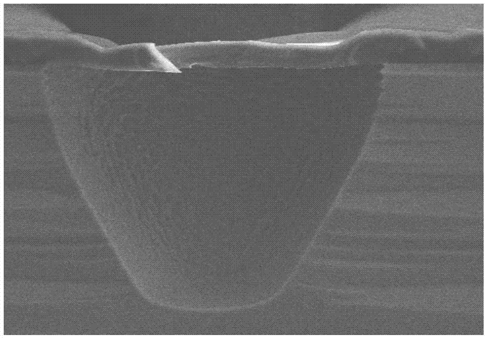
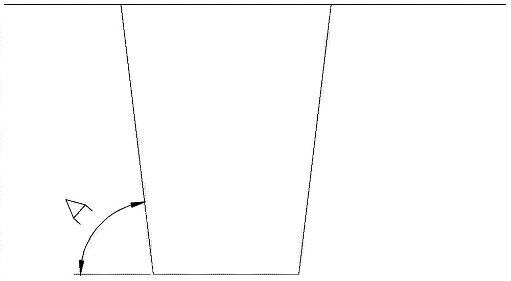
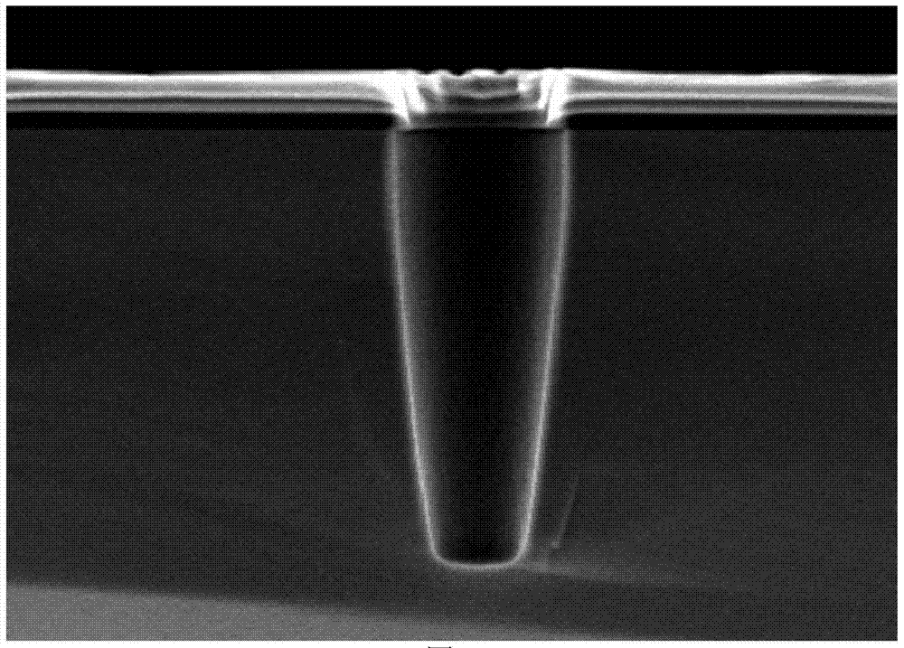
[0028] In order to enable those skilled in the art to better understand the technical solution of the present invention, the oblique hole etching method provided by the present invention will be described in detail below with reference to the accompanying drawings.

[0029] The oblique hole etching method provided by the present invention includes the following steps: feeding etching gas and auxiliary gas into the reaction chamber, and turning on the excitation power supply (such as a radio frequency power supply), the excitation power supply is used to apply excitation power to the reaction chamber, so that The etching gas in the reaction chamber is excited to form plasma; the bias power supply is turned on, and the bias power supply is used to apply bias power to the silicon wafer, so that the plasma etches the silicon wafer until it forms on the surface of the silicon wafer to be etched. Slanted holes with a predetermined etch depth. In practical applications, the above etc...


PUM


Abstract

The invention provides a method for etching oblique holes, which includes the following steps: feeding an etching gas into a reaction chamber, and turning on an excitation power supply and a bias power supply to etch oblique holes on a surface to be etched of a silicon wafer; Among them, the etching gas includes SF6 and O2; the gas flow ratio of SF6 and O2, process pressure, excitation power and bias power are set as follows: by increasing the gas flow ratio of SF6 and O2, and increasing the process pressure, excitation power and bias power to obtain the ideal oblique hole etching morphology. The oblique hole etching method provided by the present invention can not only obtain the ideal oblique hole etching morphology, that is, the inclination angle is in the range of 80-88°, the side wall is smooth and there is no bandwidth loss, and it can also improve the etching efficiency. speed, thus not only meeting the requirements of the TSV process, but also improving the process efficiency.

Description

technical field [0001] The invention relates to the technical field of microelectronics, in particular to an oblique hole etching method. Background technique [0002] As MEMS devices and MEMS systems are more and more widely used in the automotive and consumer electronics fields, and TSV through hole etching (Through Silicon Etch) technology has broad prospects in the future packaging field, dry plasma deep silicon etching process It has gradually become one of the hottest processes in the field of MEMS processing and TSV technology. The etching process of oblique holes is currently an important means to achieve TSV and packaging fields. This is because: for straight holes, especially straight holes with a certain depth-to-width ratio, it will increase the difficulty of PVD filling in the subsequent channel. And the oblique hole (the inclination angle is about 85°) is more conducive to the PVD filling in the back channel. [0003] The existing oblique hole etching method ...

Claims


Application Information

Patent Timeline
Patent Type & Authority Patents(China)
IPC IPC(8): B81C1/00
Inventor 谢秋实李成强
Owner BEIJING NAURA MICROELECTRONICS EQUIP CO LTD
Why Eureka
Try Eureka