

Chip-like electric component and method for manufacturing same
A technology of electrical components and electrical components, applied in the direction of electrical components, resistance manufacturing, resistor parts, etc.
- Summary
- Abstract
- Description
- Claims
- Application Information
AI Technical Summary
Problems solved by technology
Method used
Image

Examples
Embodiment Construction
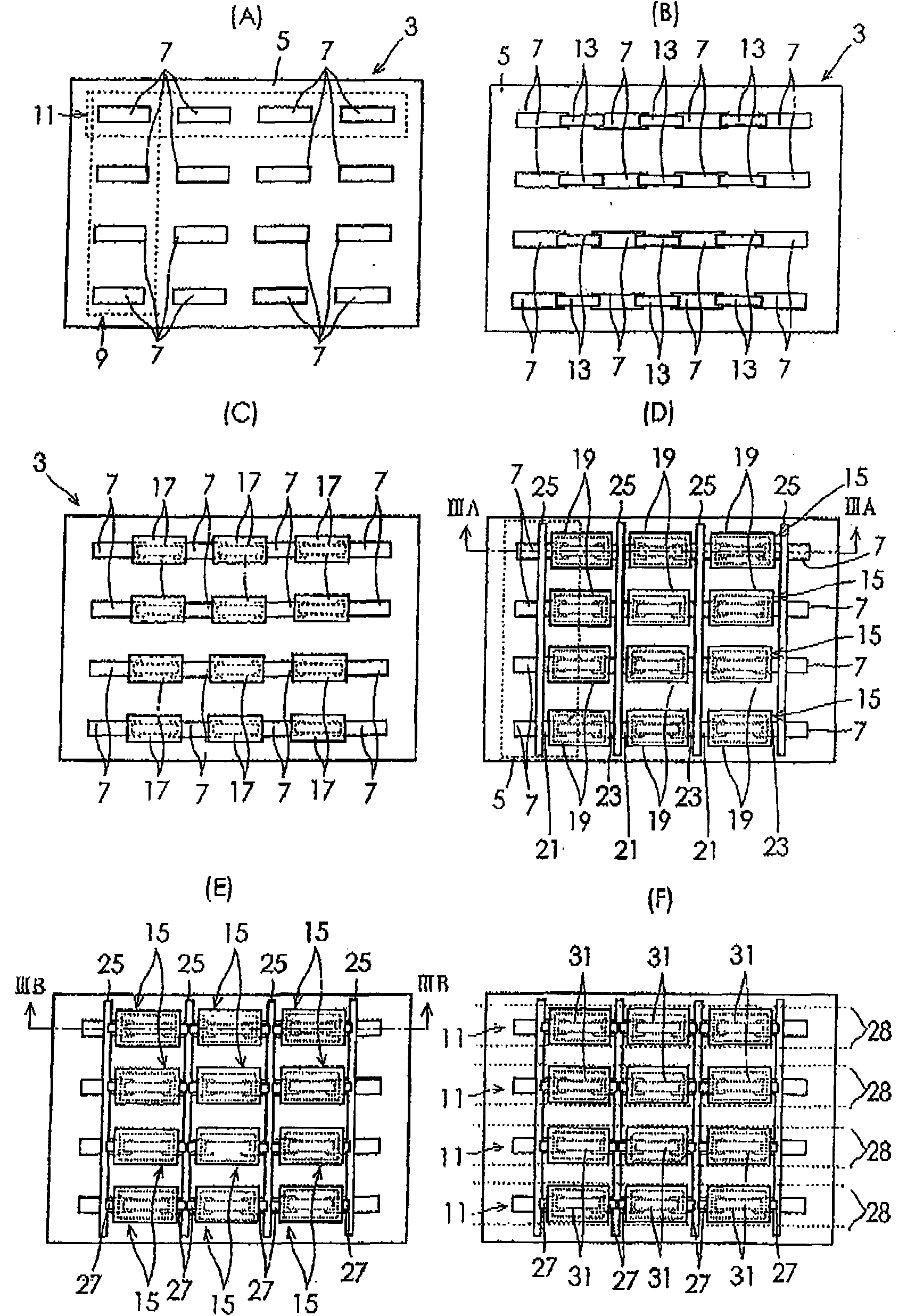
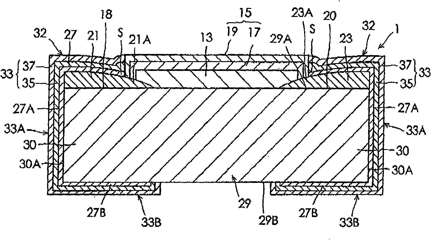
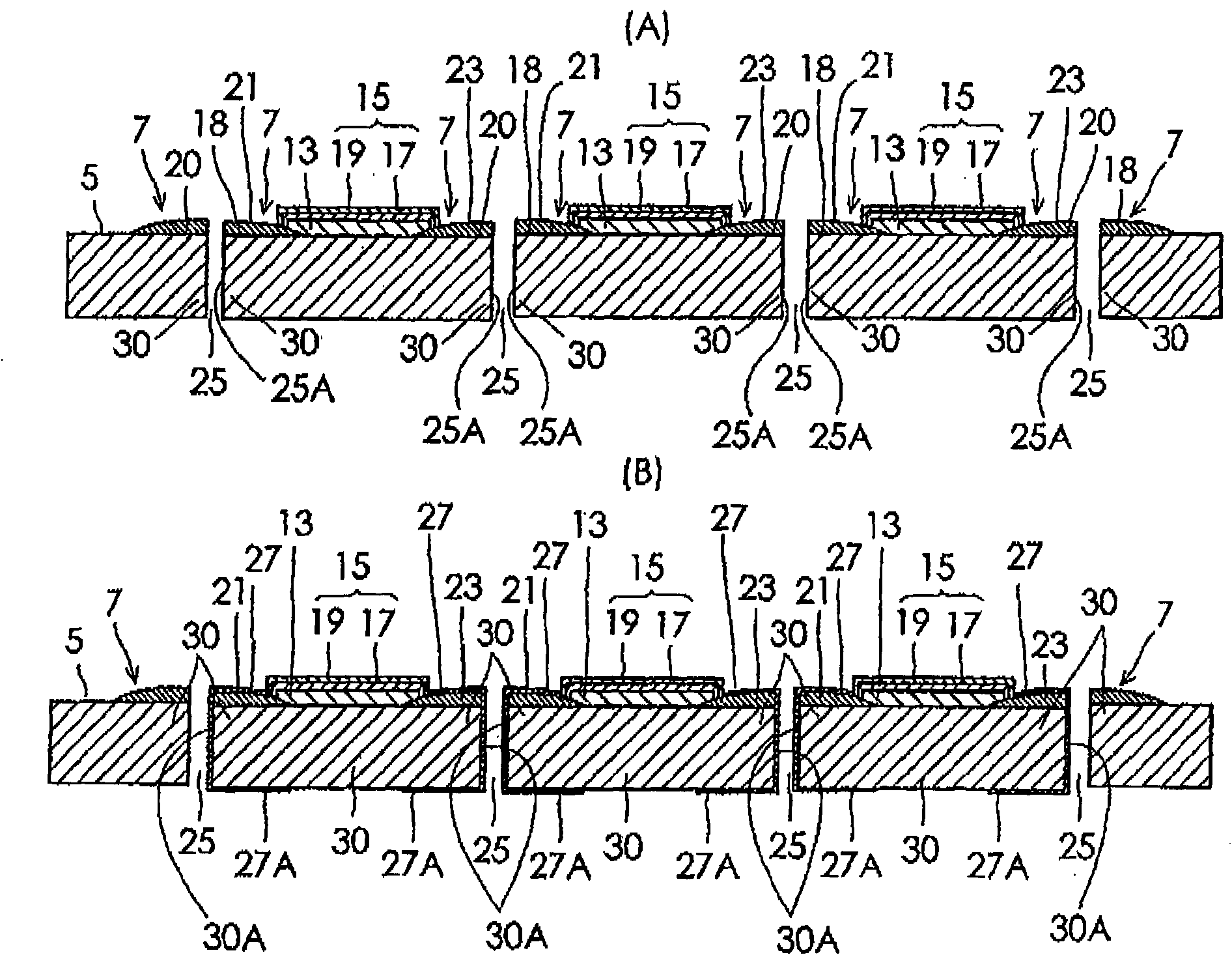
[0022] Hereinafter, embodiments of the chip-shaped electrical component of the present invention will be described in detail with reference to the drawings. figure 1 It is a cross-sectional view schematically showing the structure of a chip resistor 1 which is one type of chip-like electrical component manufactured by the manufacturing method of the chip-like electrical component of the present invention. figure 1 This is a cross-sectional view schematically shown for easy understanding, and the dimensional ratio of each part, the thickness and shape of each layer are different from those of an actual member. figure 2 (A) to (F) are shown figure 1 A process diagram of a plurality of steps in the manufacturing method of the chip resistor 1 according to the embodiment. use figure 2 process diagrams, while describing the manufacturing method of the chip resistor 1 of this embodiment, together with figure 1 The structure of the chip resistor 1 will be described.
[0023] exi...
PUM
 Abstract
Description
Claims
Application Information