Back contact electrode in cadmium telluride membrane solar cell structure and preparation method thereof

A solar cell and back contact electrode technology, applied in the field of microelectronics, can solve the problems of not considering the cost, not being able to form ohmic contacts, and affecting carrier conduction

Active Publication Date: 2011-05-25
SHANGHAI INST OF CERAMIC CHEM & TECH CHINESE ACAD OF SCI
View PDF2 Cites 17 Cited by
  • Summary
  • Abstract
  • Description
  • Claims
  • Application Information

AI Technical Summary

Problems solved by technology

[0008] The work function of CdTe is about 5.5eV, such a high work function makes it impossible to form an ohmic contact between CdTe and the existing material used as the back electrode, and there is a Schottky junction, which seriously affects t...

Method used


Image

  • Back contact electrode in cadmium telluride membrane solar cell structure and preparation method thereof
  • Back contact electrode in cadmium telluride membrane solar cell structure and preparation method thereof
  • Back contact electrode in cadmium telluride membrane solar cell structure and preparation method thereof

Examples


Embodiment 1

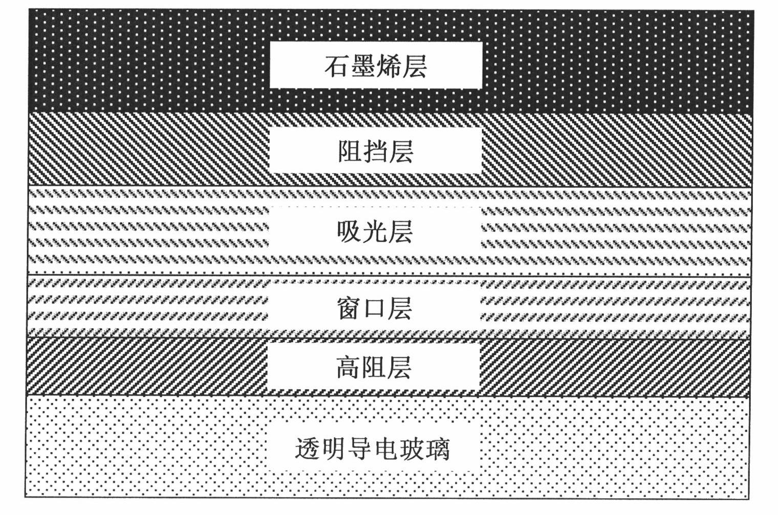
[0043] Preparation of transparent conductive layer: AZO conductive glass is prepared by sputtering method, the temperature of the glass substrate is 600°C at room temperature, the carrier gas is argon or argon-hydrogen mixed gas (where the hydrogen is less than 10%), the reaction pressure is 0.1Pa, and the gas flow rate is 5sccm (standard cubic centimeter per minute, standard cubic centimeter per minute), the power is 50W, the target distance is 5cm, where N 2 as a carrier gas. The deposition thickness is about 600nm. Obtain the transparent conductive glass ( figure 2 ).

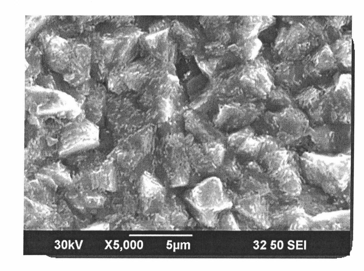
[0044] Window layer preparation: prepared by sputtering method, the temperature of the conductive glass substrate is room temperature, the reaction pressure is 0.1Pa, the power is 100W, and the target material is CdS target, where N 2 As a carrier gas, the gas flow rate was 5 sccm. The deposition thickness is about 100nm ( image 3 ).

[0045] Preparation of light-absorbing layer: prepared by sputteri...

Embodiment 2

[0049] Preparation of transparent conductive layer: LPCVD is used to deposit FTO conductive glass, the substrate temperature is 400°C, the reaction pressure is 3kPa, the reaction precursor is Tetramethyltin (TMT), Bromotrifluoromethane (CBrF3) gas provides F source, and at the same time, O 2 and N 2 , where N 2 as a carrier gas. The deposition thickness is about 500nm.

[0050] Window layer preparation: prepared by sputtering method, the temperature of the conductive glass substrate is room temperature, the reaction pressure is 0.1Pa, the power is 100W, and the target material is CdS target, where N 2 As a carrier gas, the gas flow rate is 5 sccm. The deposition thickness is about 100 nm. .

[0051] Preparation of light-absorbing layer: prepared by sputtering method, the temperature of the above substrate is 300°C, the reaction pressure is 0.1Pa, the power is 100W, argon or argon-oxygen mixed gas is used as the carrier gas, the gas flow rate is 5 sccm, the target material...

Embodiment 3

[0056] Preparation of transparent conductive layer: LPCVD is used to deposit FTO conductive glass, the substrate temperature is 400°C, the reaction pressure is 3kPa, the reaction precursor is Tetramethyltin (TMT), Bromotrifluoromethane (CBrF3) gas provides F source, and at the same time, O 2 and N 2 , where N 2 as a carrier gas. The deposition thickness is about 500nm.

[0057] Preparation of the window layer: The CdS layer was prepared by the chemical water bath method, and the reactants were ammonium acetate, cadmium acetate, ammonia water and thiourea. First, add deionized water into a sealed container, heat it to 80°C, add cadmium acetate, ammonium acetate, and ammonia water, and deposit a thickness of about 100nm.

[0058] Preparation of light-absorbing layer: prepared by sputtering method, the temperature of the above substrate is 300°C, the reaction pressure is 0.1Pa, the power is 100W, argon or argon-oxygen mixed gas is used as the carrier gas, the gas flow rate is ...


PUM

PropertyMeasurementUnit
Thicknessaaaaaaaaaa
Thicknessaaaaaaaaaa
Thicknessaaaaaaaaaa

Abstract

The invention relates to a back contact electrode in a CdTe membrane solar cell structure. The electrode comprises a transparent conductive glass layer, a window layer, a light absorbing layer and a blocking layer and is characterized in that: a graphene membrane layer serving as the back contact electrode is prepared on the back face of an anti-insertion layer; and the thickness of the graphene layer is between 0.1 mu m and 1 millimeter. A preparation method of the back contact electrode comprises preparation of the transparent conductive glass layer, preparation of the window layer, preparation of the light absorbing layer and preparation of the blocking layer and is characterized by comprising the following steps of: adding an adhesive into graphene so as to prepare graphene slurry; and preparing the graphene slurry into a graphene layer. The back contact electrode and the preparation method have the advantages that: a process adopted by the preparation method is compatible with the conventional CdTe cell process, and a new measure for realizing a low-cost, high-performance and large-scale CdTe cell is provided.

Description

technical field [0001] The invention relates to a back contact electrode in a cadmium telluride thin-film solar cell structure and a preparation method thereof, more precisely relates to a graphene applied to a cadmium telluride battery contact back electrode and a preparation method thereof, and belongs to the field of microelectronic technology. Background technique [0002] As mankind enters the 21st century, environmental pollution and energy shortages have increasingly restricted the sustainable development of society. Renewable energy technologies such as solar energy represent the development direction of clean energy. As the most ideal feature of sustainable development, solar photovoltaic Power generation will enter the human energy structure and become an important part of basic energy. my country has also included it in the national medium and long-term scientific and technological development plan as an important basic condition for building a new society with harm...

Claims


Application Information

Patent Timeline
IPC IPC(8): H01L31/0224H01L31/18
CPCY02P70/50
Inventor 黄富强梁军李德增林天全
Owner SHANGHAI INST OF CERAMIC CHEM & TECH CHINESE ACAD OF SCI
Why Eureka
Try Eureka