Light emitting diode and manufacturing process thereof

A technology for light-emitting diodes and manufacturing processes, applied in electrical components, electrical solid-state devices, circuits, etc., can solve problems such as increased manufacturing costs, reduced manufacturing efficiency, and inability to perform rapid drilling, so as to reduce manufacturing costs and reduce substrate waste. , The effect of improving the utilization rate of the substrate

Inactive Publication Date: 2011-05-25
ZHANJING TECH SHENZHEN +1
View PDF2 Cites 13 Cited by
  • Summary
  • Abstract
  • Description
  • Claims
  • Application Information

AI Technical Summary

Problems solved by technology

However, when drilling, it is necessary to control not to drill through the upper electrode portion 133a to form the blind hole, and to use the upper electrode portion 133a as a barrier to prevent the glue forming the covering layer from flowing into the hole. The thickness of the electrode part 133a is extremely thin, so it is necessary to use a more precise tool to control the depth of the drilled hole. In this way, due to the use of a more precise tool and equipment, the manufacturing cost is increased. In order to control the drilled hole depth, it is impossible to perform fast drilling, which will also make the manufacturing process difficult. Prolonged time reduces manufacturing efficiency

Method used


Image

  • Light emitting diode and manufacturing process thereof
  • Light emitting diode and manufacturing process thereof
  • Light emitting diode and manufacturing process thereof

Examples


Embodiment Construction

[0038] A first preferred embodiment of the manufacturing process of the light-emitting diode of the present invention includes the following steps:

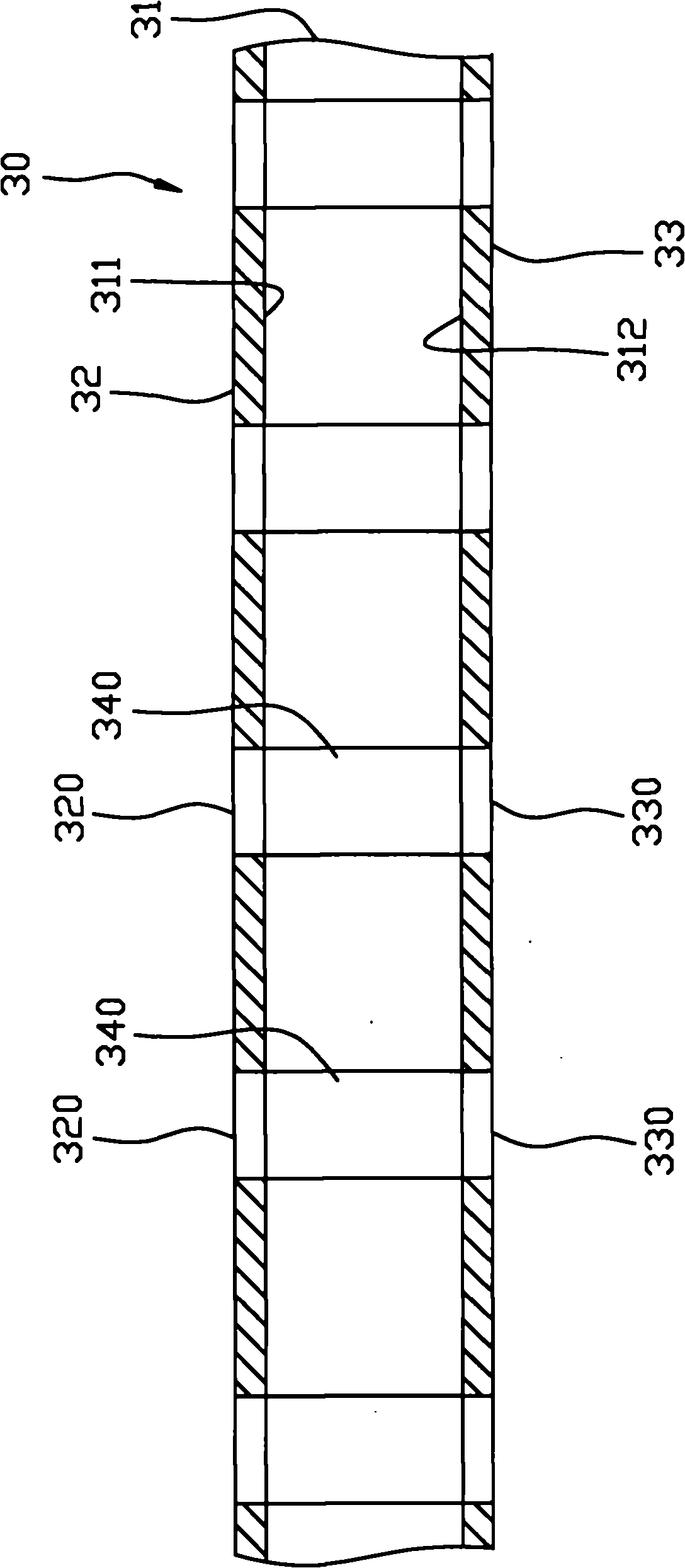
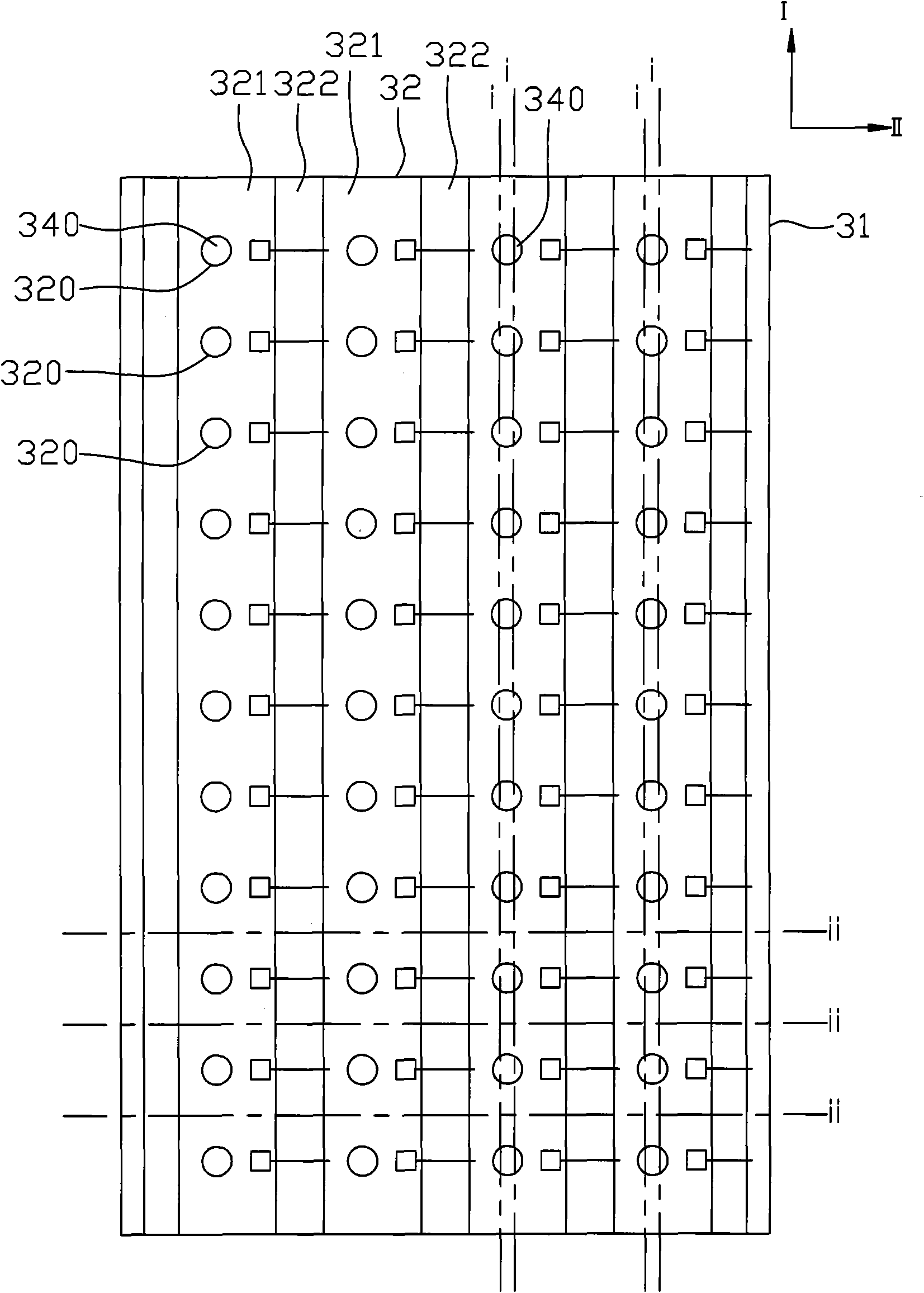
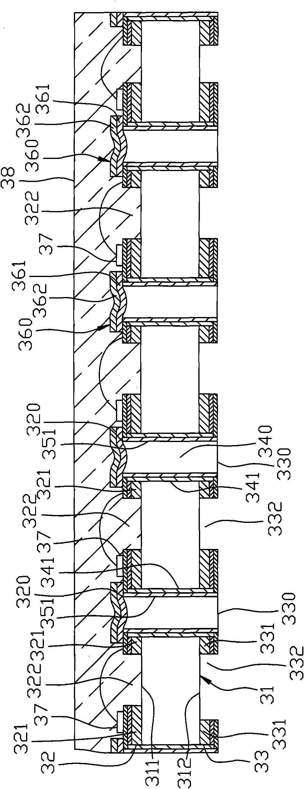
[0039] refer to figure 1 , figure 2 and image 3 , step 301 is to provide a substrate assembly 30, the substrate assembly 30 has a substrate 31, a plurality of upper electrode portions 321 arranged on an upper surface 311 of the substrate 31 at intervals along a first direction I, a plurality of interlayers The upper etched portion 322 between the upper electrode portions 321, a plurality of lower electrode portions 331 arranged at intervals along the first direction I on the lower surface 312 of the substrate 31, and a plurality of lower electrode portions 331 interposed between the lower electrode portions 331 The lower etching portion 332, a plurality of holes 340 spaced apart and penetrating the substrate 31 and the upper and lower electrode portions 321, 331, the holes 340 are respectively defined in the upper and lower ...


PUM


Abstract

The invention discloses a light emitting diode (LED) and a manufacturing process thereof. The manufacturing process comprises the following steps of: providing a substrate assembly, wherein the substrate assembly is provided with a substrate, a plurality of upper and lower electrode parts arranged on the upper and lower surfaces of the substrate respectively, a plurality of upper and lower etching parts positioned between the upper and lower electrode parts respectively, a plurality of holes formed at intervals and passing through the substrate and the upper and lower electrode parts, and a plurality of connecting electrode parts arranged on the inner circumference walls of the defined holes respectively; and forming a plurality of blocking units for closing multiple upper openings of theupper electrode parts respectively, finally arranging an LED chip between the two upper electrode parts, forming a coverage layer, and obtaining the LED by cutting. The manufacturing process can promote the utilization rate of the substrate, and can perform two times of molding so as to enhance the luminous strength of the LED.

Description

technical field [0001] The invention relates to a light-emitting diode and its manufacturing process, in particular to a light-emitting diode suitable for use in optoelectronic products and its manufacturing process. Background technique [0002] The existing manufacturing process of light-emitting diodes has the following steps: [0003] Step 101 is to firstly form a plurality of spaced and hollowed-out channels on a substrate along a first direction, and respectively form a conductive upper and a lower electrode layer on an upper surface and a lower surface of the substrate, each channel Both are formed by two side wall surfaces parallel to the first direction, and two end wall surfaces connected between the side wall surfaces. [0004] Step 102 is to etch the upper and lower electrode layers respectively to form upper and lower electrode parts arranged along the first direction, and a plurality of upper and lower etched parts respectively interposed between the upper and...

Claims


Application Information

Patent Timeline
Patent Type & Authority Applications(China)
IPC IPC(8): H01L33/48H01L33/62
CPCH01L24/97H01L2224/48091H01L2224/48227H01L2924/12041H01L2924/00014H01L2924/00
Inventor 林升柏张超雄曾文良
Owner ZHANJING TECH SHENZHEN
Why Eureka
Try Eureka