Laminated differential inductor with top layer metal and second layer metal of equal thickness

A top-layer metal and differential inductance technology, applied in the field of microelectronics, can solve the problem of large area of ​​inductance, and achieve the effect of improving inductance value, Q value and inductance value

Inactive Publication Date: 2011-06-08
SHANGHAI HUA HONG NEC ELECTRONICS
View PDF0 Cites 5 Cited by
  • Summary
  • Abstract
  • Description
  • Claims
  • Application Information

AI Technical Summary

Problems solved by technology

However, in order to obtain a large inductance value, the inductor of the traditional differential structure still needs a relatively large area

Method used


Image

  • Laminated differential inductor with top layer metal and second layer metal of equal thickness
  • Laminated differential inductor with top layer metal and second layer metal of equal thickness
  • Laminated differential inductor with top layer metal and second layer metal of equal thickness

Examples


Embodiment Construction

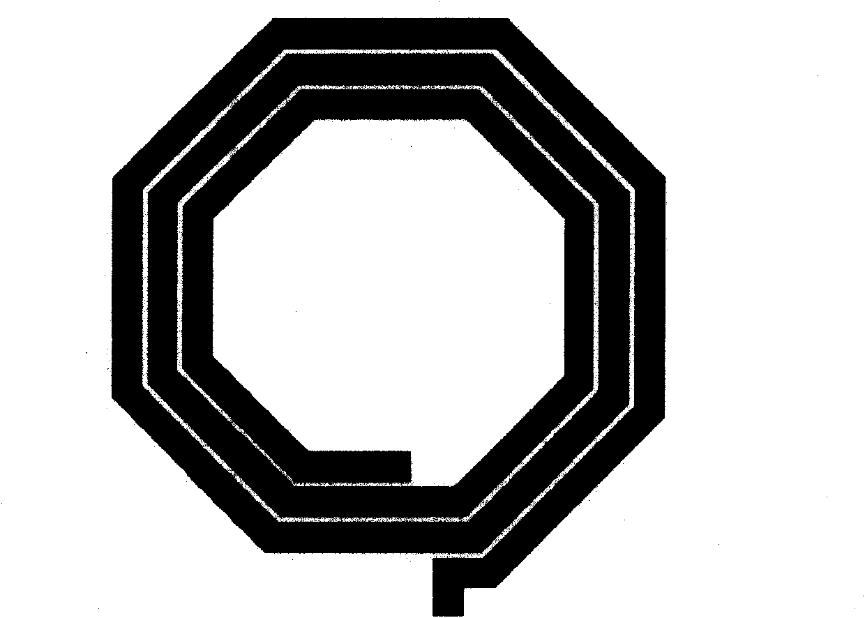
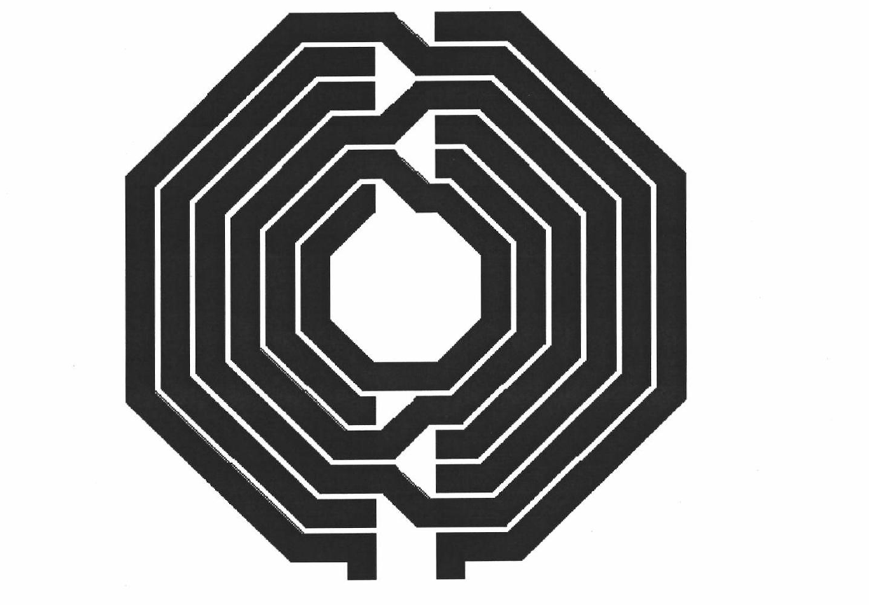
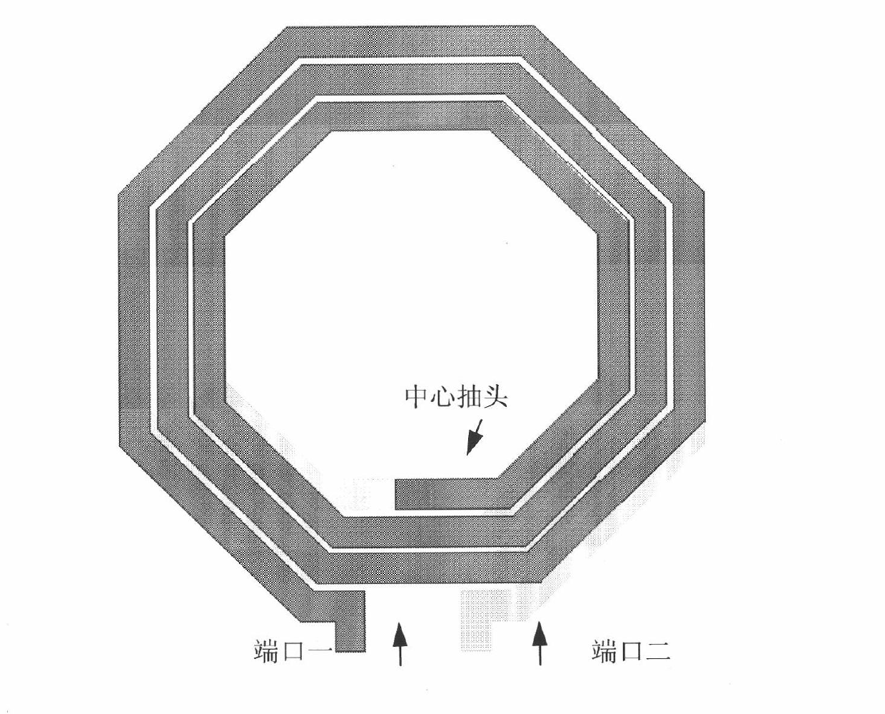
[0016] The stacked differential inductor with the same thickness of the top layer and the second top layer metal of the present invention; it is a multi-layer structure, including: the upper and lower layer metal coils, the upper and lower layer metal coils have symmetrical patterns, and the thickness of the upper and lower layer metal coils is equal; the metal coils There is an inductance port; the inductance starts from one inductance port, spirally winds to the innermost end on the first layer of metal coils, and then connects to another layer of metal coils through interlayer through holes; the other layer of metal coils is screwed again The wire is wound to the outermost end, and the upper and lower layer metal coils are interconnected through interlayer through holes.

[0017] In more detail, the stacked differential inductance planar structure with the same thickness of the top layer and the second top layer metal described in the present invention (take two layers of me...


PUM


Abstract

The invention discloses a laminated differential inductor with a top layer metal and a second layer metal of equal thickness. The laminated differential inductor has a multilayer structure and comprises an upper layer metal coil and a lower layer metal coil, wherein the upper layer metal coil and the lower layer metal coil have symmetric patterns and equal thickness; the metal coils are provided with inductance ports; in the inductor, the first layer of metal coil is spirally wound to the innermost end from one inductance port and then is connected with the other layer of metal coil through an interlayer through hole; the other layer of metal coil is spirally wound to the outermost end; and the upper layer metal coil is interconnected with the lower layer metal coil through the interlayer through hole. Since the mutual inductance between the symmetric upper layer metal and lower layer metal is fully utilized, the inductance of the inductor is effectively improved under the same area condition compared with the inductance of the conventional differential inductor. Both quality (Q) factor and inductance are obviously improved under the same area condition.

Description

technical field [0001] The invention relates to the field of microelectronics, in particular to a differential inductor using a stacked structure. Background technique [0002] At present, a large number of passive devices are included in integrated circuits, among which on-chip inductors are a very important one, and on-chip inductors are one of the important components of radio frequency CMOS / BiCMOS integrated circuits. In typical wireless products, inductive components have a significant impact on the overall RF performance. Therefore, the design and analysis of these inductive components have also been extensively studied. As the core component of the RF circuit, the inductor can usually affect the overall performance of the entire circuit. At present, on-chip inductors with high quality factors are widely used in RF circuit modules such as voltage-controlled oscillators and low-noise amplifiers. The stacked on-chip inductor greatly reduces the chip area and reduces t...

Claims


Application Information

Patent Timeline
Patent Type & Authority Applications(China)
IPC IPC(8): H01F17/00H01F37/00H01F27/28H01F27/29H01F41/06H01L23/522
Inventor 邱慈云徐向明蔡描王生荣
Owner SHANGHAI HUA HONG NEC ELECTRONICS
Why Eureka
Try Eureka