LED chip jointing device

A technology of LED chips and bonding devices, applied in the direction of electrical components, electrical components, circuits, etc., can solve the problems of delaying production time, undisclosed structure, reducing productivity, etc.

Inactive Publication Date: 2011-06-08
TOP ENG CO LTD
View PDF4 Cites 7 Cited by
  • Summary
  • Abstract
  • Description
  • Claims
  • Application Information

AI Technical Summary

Problems solved by technology

[0012] However, since the existing LED chip bonding apparatus 10 attaches the LED chip C to the lead frame LF during the reciprocating movement of the head unit 41 between the wafer stage 30 and the feed rail 21, relative longer time
That is, the long path...

Method used


Image

  • LED chip jointing device
  • LED chip jointing device
  • LED chip jointing device

Examples


Embodiment approach 1

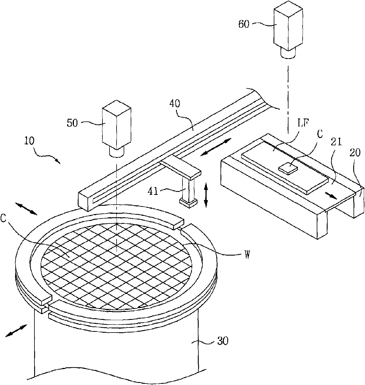
[0033] figure 2 is a perspective view illustrating the LED chip bonding apparatus according to the first embodiment of the present invention. image 3 Yes figure 2 Schematic diagram of the LED chip bonding setup. Figure 4 is icon figure 2 A perspective view of another example of the main body.

[0034] like figure 2 and image 3 As shown, the LED chip bonding apparatus A according to the first embodiment of the present invention includes: a wafer holder 100 on which a wafer W having an LED chip C is installed, and it can be arranged along a plane perpendicular to each other along axes (hereinafter referred to as For "X-axis" and "Y-axis") movement; lead frame holder 200, on which lead frame LF is positioned, and which can move along two orthogonal axes on a plane parallel to the plane on which the wafer holder moves; LED chip transfer unit 300, which can rotate around an axis (hereinafter referred to as "Z axis") perpendicular to the plane where the wafer carrier mo...

Embodiment approach 2

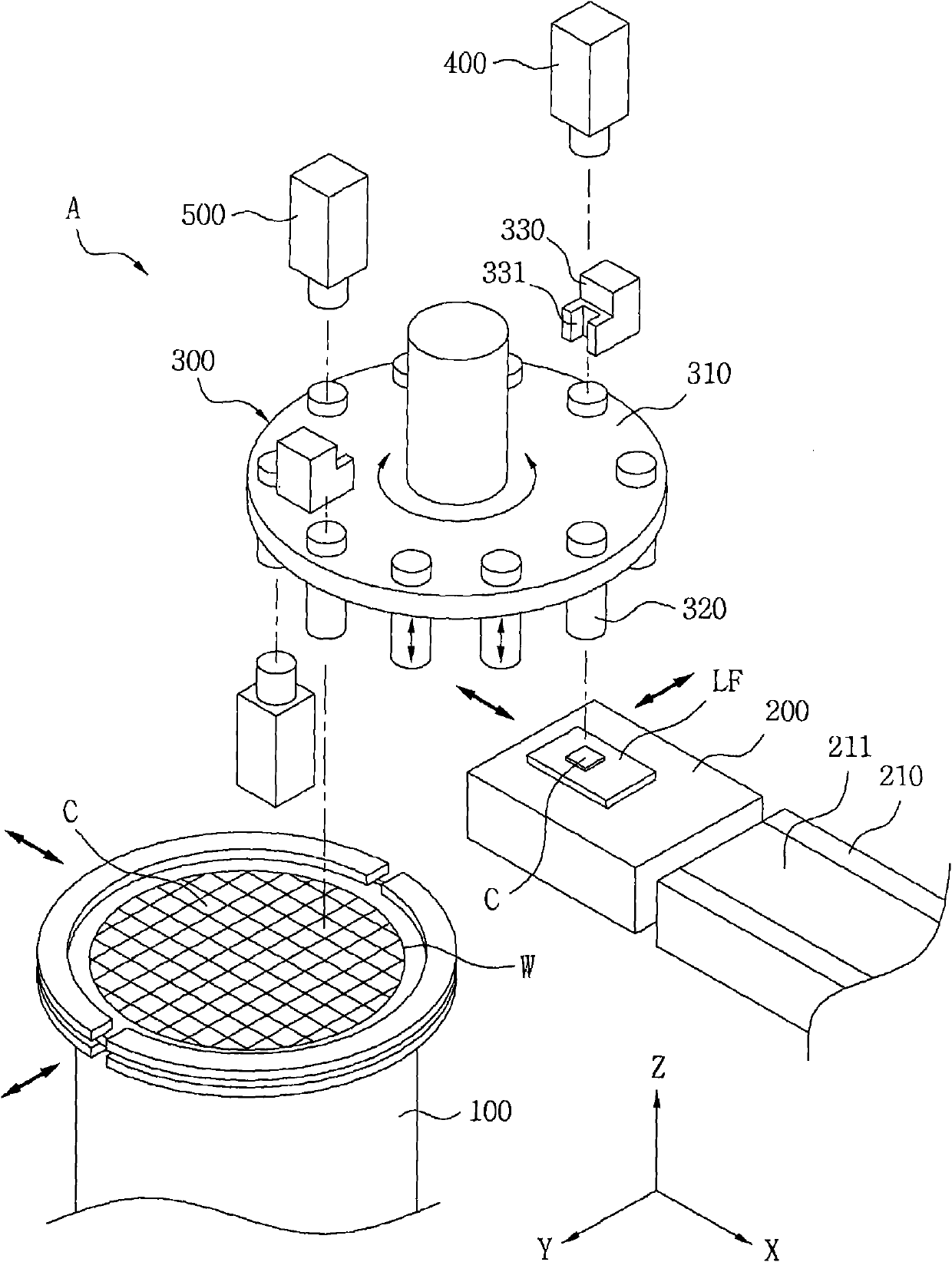
[0061] Figure 5 is a perspective view illustrating an LED chip bonding apparatus according to a second embodiment of the present invention.

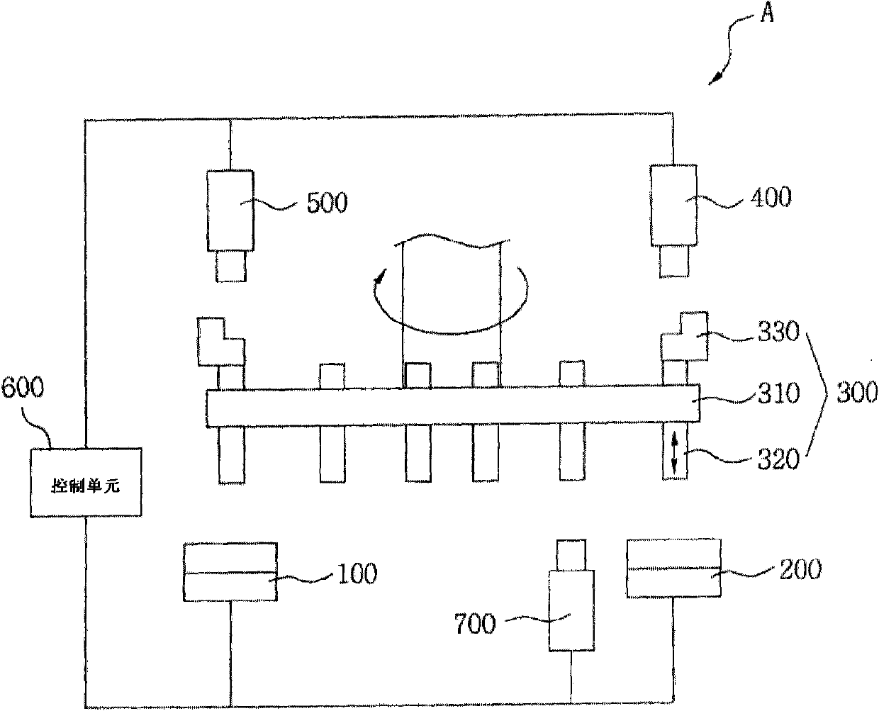
[0062] like Figure 5 As shown, the LED chip bonding apparatus A' according to the second embodiment of the present invention includes: a wafer holder 100; a lead frame holder 200; the LED chip transfer unit 300 ′; the first vision unit 400 configured to recognize the position information of the lead frame LF and the second vision unit 500 configured to recognize the position information or setting state of the LED chip C; and the control unit 600 .

[0063] The LED chip transfer unit 300' includes: a main body 310' movable along the Z axis and rotatable around the Z axis; and a plurality of head devices 320' attached to the circumference of the main body 310' at equal intervals.

[0064] The main body 310' itself is moved in the Z-axis direction by a pressing unit such as a pneumatic cylinder or a hydraulic cylinder.

[0065] As des...


PUM


Abstract

The invention discloses an LED chip jointing device including a wafer support which has a wafer with an LED chip installed thereon and can move along the orthogonal axes on a plane; a lead wire frame support which has a lead wire frame positioned thereon and can move along two orthogonal axes on a plane parallel to the plane where the wafer support moves; an LED chip transferring unit which rotates about an axis perpendicular to the plane where the wafer support moves so as to transfer LED chips on the wafer support onto the lead wire frame support ; a first video unit constituted to identify location information of the lead wire frame; a second video unit constituted to identify location information of an LED chip about to depart from the wafer support or setting state of an LED chip in the wafer; and a control unit which is constituted to adjust the wafer support and the lead wire frame support based on the information of the first video unit and the second video unit so as to align the joint position of the LED chip and the lead wire frame. The LED chip transferring unit picks up the LED chip and attaches the LED chip to the lead wire frame.

Description

[0001] Cross References to Related Applications [0002] This application claims the priority benefit of Korean Patent Application No. 2009-0119536 filed on Dec. 04, 2009, the disclosure of which is incorporated herein by reference in its entirety. technical field [0003] The present invention relates to an LED chip bonding apparatus, and more particularly, to an LED chip bonding apparatus that shortens the time period for picking up an LED chip and attaching the LED chip to a lead frame, thereby improving productivity. Background technique [0004] In general, LEDs are manufactured through the following steps: a bonding process of bonding a wafer having a plurality of LED chips to a bonding sheet; a dicing process of individualizing the LED chips by dicing the wafer bonded to the bonding sheet; The die separating process of separating the LED chip from the bonding sheet; the die bonding process of bonding the LED chip separated from the bonding sheet to the lead frame; the...

Claims


Application Information

Patent Timeline
IPC IPC(8): H01L33/48H01L33/62
CPCH01L33/48H05K13/0015H05K13/04H05K13/08
Inventor 张贤锡李闵泂李悳镐朴敏奎
Owner TOP ENG CO LTD
Why Eureka
Try Eureka