
Preparation method of silicon-based composite substrate for electronic device

A technology for electronic devices and composite wafers, applied in the field of preparing silicon-based diamond film composite substrates for electronic devices, can solve the problems of chipping of silicon wafers, slow deposition rate, poor quality, etc., and can correct deformation, prevent etching, reduce small deformation effect

Active Publication Date: 2013-04-03
UNIV OF SCI & TECH BEIJING
View PDF0 Cites 0 Cited by
  • Summary
  • Abstract
  • Description
  • Claims
  • Application Information

AI Technical Summary

Problems solved by technology

In order to have both semiconductor performance and high heat dissipation characteristics at the same time, it has been proved that the diamond film has a certain thickness, generally greater than 25 microns. Although the microwave CVD method deposits diamond films with high quality, the deposition rate is slow and the efficiency is low. Large-area also more difficult
Hot wire CVD and hot cathode methods can achieve large areas but relatively poor quality
[0003] Although the most basic and most suitable choice for depositing diamond films on silicon substrates, the deposition of diamond films on silicon substrates by plasma spraying has been difficult to achieve because the silicon wafers are easily cracked due to the thermal shock of the plasma arc.

Method used


Image

  • Preparation method of silicon-based composite substrate for electronic device
  • Preparation method of silicon-based composite substrate for electronic device

Examples


Embodiment 1

[0024] The diamond film is deposited on a silicon substrate with a thickness of 3 inches and a thickness of 4 mm by the plasma jet method. The gas flow rates in the deposition parameters are hydrogen 6L, argon 3L, and methane 90Sccm, and the power parameters are arc current 95A, respectively. The arc voltage is 105V, the deposition temperature is 930°C, the distance between the anode and the silicon substrate is 50mm, the deposition time is 5 hours, and the thickness of the deposited diamond film is 56 microns; then the silicon-based diamond film composite sheet is placed in reverse for arc plasma treatment, The processing parameters are hydrogen 6L, argon 3L, arc current 105A, arc voltage 103V, substrate temperature 950°C, distance between anode and silicon-based diamond composite sheet 50mm, and processing time 10 minutes to obtain silicon-based diamond film composite The thickness of the diamond film in the chip is 56 microns; after taking it out, it is placed in a vacuum he...

Embodiment 2

[0026] The present invention uses the plasma jet method to deposit the diamond film on a silicon substrate with a thickness of 5 inches and 4 millimeters. The gas flow rates in the deposition parameters are respectively 4 L of hydrogen, 6 L of argon, and 120 Sccm of methane, and the parameters of the power supply are arc current respectively. 130A, arc voltage 101V, deposition temperature 1100°C, distance between anode and silicon substrate 60mm, deposition time 6.5 hours, thickness of deposited diamond film 100 microns; take it out and place it in a vacuum heat treatment furnace for annealing to eliminate Residual stress reduces deformation in further processing, vacuum limit is 5×10 -3 Pa, the heating temperature is 1050°C, the holding time is 1.5 hours, the cooling rate is 50°C / hour, and it cools with the furnace when it reaches 700°C. Then the diamond growth surface of the silicon-based diamond film composite sheet is ground and polished. After polishing, the thickness of ...

Embodiment 3

[0028] The present invention uses the plasma jet method to deposit the diamond film on a silicon substrate with a thickness of 2 inches and a thickness of 15 mm. The gas flow rates in the deposition parameters are respectively 7 L of hydrogen, 3 L of argon, and 100 Sccm of methane, and the parameters of the power supply are arc current respectively. 95A, arc voltage 105V, deposition temperature 980°C, distance between anode and silicon substrate 80mm, deposition time 5 hours, thickness of deposited diamond film 65 microns. Then reversely place the silicon-based diamond film composite sheet for arc plasma treatment. The processing parameters are hydrogen 6L, argon 3L, arc current 105A, arc voltage 103V, substrate temperature 950°C, and the anode and silicon-based diamond composite sheet. The distance is 50mm and the processing time is 10 minutes. After taking it out, place it in a vacuum heat treatment furnace for annealing treatment to eliminate residual stress and reduce defo...


PUM

PropertyMeasurementUnit
diameteraaaaaaaaaa
thicknessaaaaaaaaaa
thicknessaaaaaaaaaa

Abstract

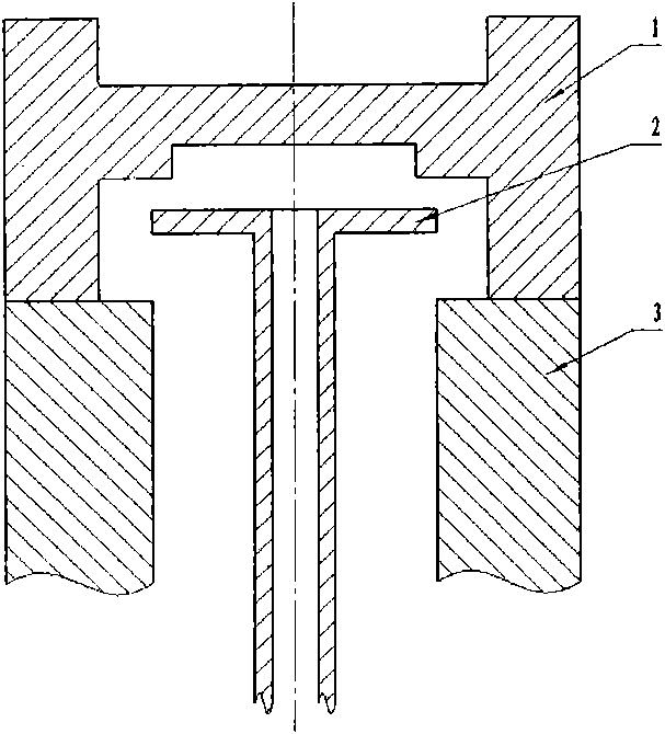
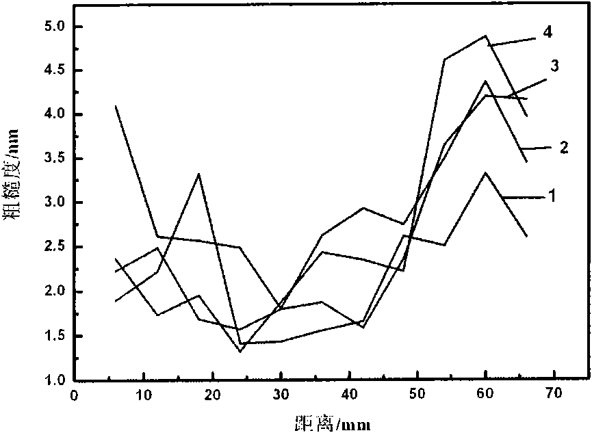
The invention belongs to the technical field of the preparation of a base material for an electronic device, and specifically provides a method for preparing a silicon-based diamond film composite substrate for an electronic device. The method comprises the following steps: using a silicon substrate with a diameter of 2-8 inches and a thickness of 4-20 millimeters as a matrix for deposition; placing onto a specially-designed stepped heat-conducting cooling body deposition platform; introducing a gaseous mixture of hydrogen gas, argon gas and methane; depositing a diamond film with vacuum arc plasma; relieving the stress of the silicon-based diamond composite substrate; grinding or polishing until the surface roughness is less than 5nm; and cutting to obtain the silicon-based diamond film composite substrate composed of the diamond film with a required thickness and the composite substrate. By using the plasma injection method to deposit the high-quality diamond film on the silicon substrate at a high speed and carrying out deformation correction and stress relieving based on plasma arc and vacuum heat treatment, the invention avoids the possible breakage of the composite substratein the grinding and polishing process, and can obtain the practical silicon-based composite substrate.

Description

technical field [0001] The invention belongs to the technical field of preparing matrix materials for electronic devices, and in particular provides a method for preparing silicon-based diamond film composite substrates for electronic devices. Background technique [0002] CVD diamond film has excellent properties and has broad application prospects in the fields of mechanics, heat, optics, acoustics, electronics and semiconductors, among which the most striking is the application in semiconductors. Diamond has a wide band gap (5.5eV), high carrier mobility, low dielectric constant (5.7), strong radiation resistance, and high breakdown field strength (3.5×10 6 V / cm) and high electron saturation velocity (2.5×10 7 cm / s), which makes it possible to use diamond to make high-frequency and high-power semiconductor devices, which work under harsh conditions such as high temperature and strong radiation. At the same time, its high thermal conductivity can be used as a heat sink f...

Claims


Application Information

Patent Timeline
Patent Type & Authority Patents(China)
IPC IPC(8): C23C14/32C23C14/06C23C14/58
Inventor 李成明陈良贤张营营刘金龙黑立富吕反修
Owner UNIV OF SCI & TECH BEIJING
Learn More