Semiconductor structure with channel stress layer and forming method thereof

A technology of stress layer and semiconductor, applied in the direction of semiconductor devices, semiconductor/solid-state device manufacturing, transistors, etc., can solve the problems of complex structure, unsuitable for mainstream technology, etc., to increase mobility, reduce diffusion/intrusion, and improve driving current Effect

Inactive Publication Date: 2011-06-29
INST OF MICROELECTRONICS CHINESE ACAD OF SCI
View PDF1 Cites 12 Cited by
  • Summary
  • Abstract
  • Description
  • Claims
  • Application Information

AI Technical Summary

Problems solved by technology

[0003] The disadvantage of the existing technology is that although the above application discloses a solution to improve the mobility of carriers through stress film coating, although it can improve the mobility of carriers, its structure is complicated and not suitable for the current mainstream technology.

Method used


Image

  • Semiconductor structure with channel stress layer and forming method thereof
  • Semiconductor structure with channel stress layer and forming method thereof
  • Semiconductor structure with channel stress layer and forming method thereof

Examples


Embodiment Construction

[0022] The embodiments of the present invention will be described in detail below. Examples of the embodiments are shown in the accompanying drawings, wherein the same or similar reference numerals indicate the same or similar elements or elements with the same or similar functions. The embodiments described below with reference to the accompanying drawings are exemplary, and are only used to explain the present invention, and cannot be construed as limiting the present invention.

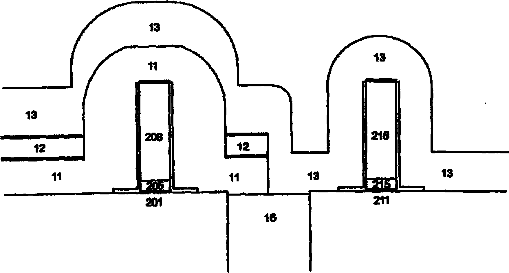
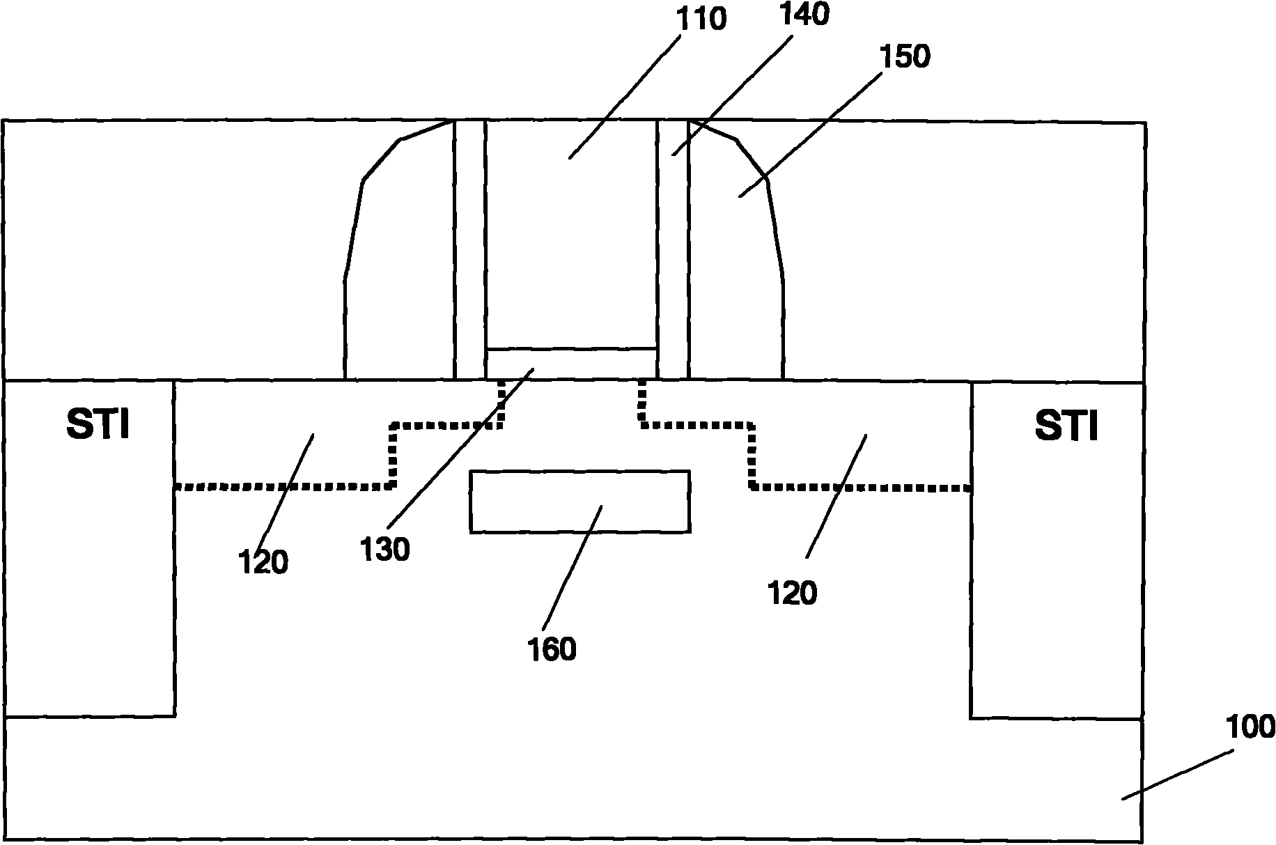
[0023] The present invention mainly lies in that an embedded stress layer is formed in the channel under the gate, and the embedded stress layer can effectively increase the mobility of carriers, thereby improving the driving current of the transistor. Such as figure 2 Shown is a structural diagram of a semiconductor structure with a channel stress layer formed in an embodiment of the present invention. The semiconductor structure includes a substrate 100 and a gate dielectric layer 130 formed on the...


PUM


Abstract

The invention provides a semiconductor structure with a channel stress layer and a forming method thereof. The semiconductor structure comprises a substrate, a grid dielectric layer formed on the substrate, a grid formed on the grid dielectric layer, a source and a drain which are formed in the substrate and positioned on two sides of the grid, one or more side walls formed on the grid dielectric layer and two sides of the grid, and an embedded stress layer which is formed below the grid and is positioned in the substrate. Due to the embedded stress layer which is arranged in a channel below the grid, the mobility of a carrier can be effectively improved; therefore, the driving current of a transistor is improved. In addition, lower thermal budget is present in the process flow of forming the embedded stress layer; therefore, the semiconductor structure contributes to keeping a higher stress level in the channel area. Moreover, besides advantage of stress, the embedded stress layer in the channel can reduce boron (B) diffusion / intrusion in heavy-doped source and drain regions.

Description

Technical field [0001] The present invention relates to the technical field of semiconductor manufacturing, in particular to a semiconductor structure formed with a channel stress layer and a method for forming the same. Background technique [0002] The performance and cost requirements of integrated circuits have led to a sharp reduction in the size of integrated circuit components, and the proximity of various devices on the chip has been increasing. As the specifications of integrated circuit components continue to decrease, many improvements have been made to the design of integrated circuit transistors in order to maintain the performance of these components at an appropriate level. For example, lightly doped structure (LDD), halo (halo) doping and graded impurity distribution are used to reduce short channel and breakdown effects. An important factor in maintaining proper performance in a field-effect transistor is carrier mobility, which affects the amount of current or ...

Claims


Application Information

Patent Timeline
Patent Type & Authority Applications(China)
IPC IPC(8): H01L29/78H01L29/10H01L21/336
CPCH01L29/7833H01L21/26506H01L29/66545H01L29/6659H01L29/6656H01L29/7849
Inventor 骆志炯朱慧珑尹海洲
Owner INST OF MICROELECTRONICS CHINESE ACAD OF SCI
Why Eureka
Try Eureka