

Integrated wafer level package
A package and wafer technology, applied in the direction of electrical components, impedance networks, etc., can solve the problems of increasing process complexity, manufacturing cost, and infeasibility
- Summary
- Abstract
- Description
- Claims
- Application Information
AI Technical Summary
Problems solved by technology
Method used
Image

Examples
example 1
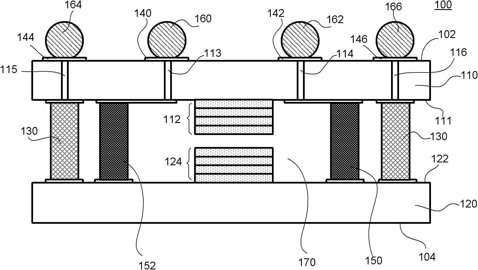
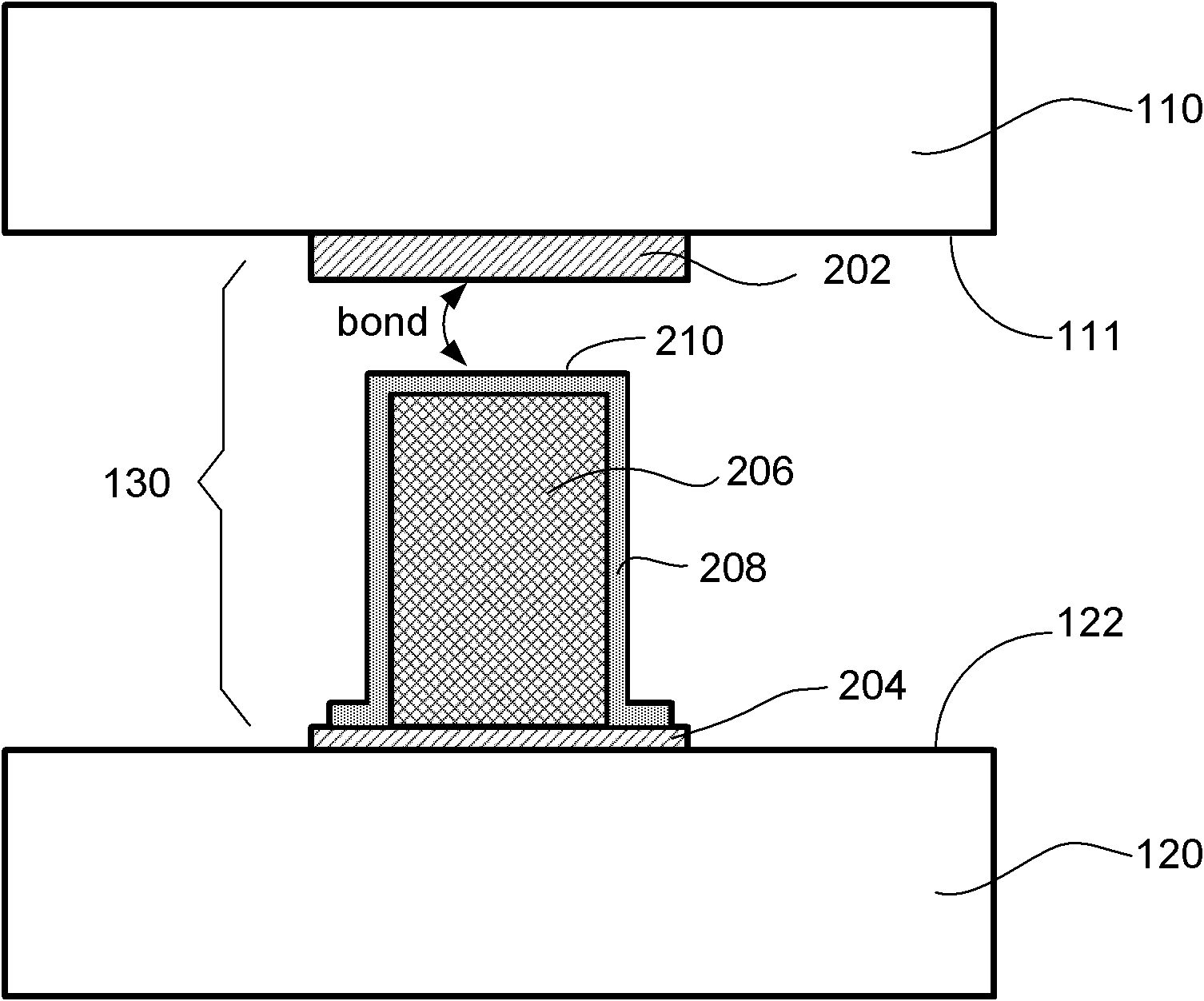
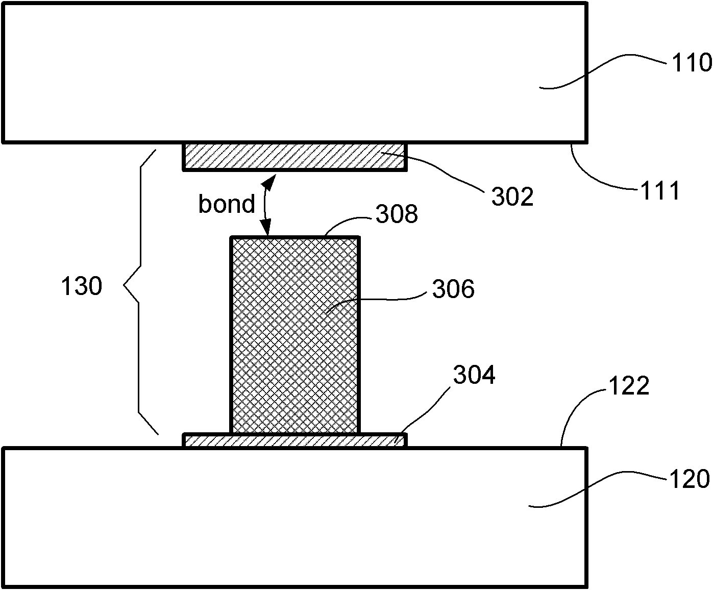
[0108] Such as figure 1 As shown, the integrated wafer level package 100 is an example obtained according to the present invention. As a typical specific example, the integrated wafer-level package 100 includes a first wafer 110, a second wafer 120, a first bulk acoustic wave filter 112, a second bulk acoustic wave filter 124, and a sealing ring 130. The first wafer 110 has a first surface 102 and a corresponding second surface 111. The second wafer 120 has a first surface 122 and a corresponding second surface 104. The first wafer 110 and the second wafer 120 are separated by a certain distance. The second surface 111 of the first wafer 110 and the first surface 122 of the second wafer 120 face each other, thereby forming a gap between the two surfaces. First distance. The first integrated acoustic wave filter 112 is fabricated on the second surface 111 of the first wafer 110, and the second bulk acoustic wave filter 124 is fabricated on the first surface 122 of the second w...
example 2
[0122] In another example, as described in Example 1, a large number of integrated wafer-level packages are stacked vertically, and each wafer-level package is connected to the adjacent wafer-level package through a second sealing ring. The packages are glued together. This can reduce more plane area.
[0123] Figure 8 It is a vertically integrated dual-band duplexer in a wafer-level package. The integrated wafer-level package 800 includes a first wafer 802, a second wafer 808, a first bulk acoustic wave filter 828, and a second bulk acoustic wave filter 830. The first wafer 802 has a first surface 804 and a corresponding second surface 806. The second wafer 808 has a first surface 810 and a corresponding second surface 812. The first wafer 802 and the second wafer 808 are separated by a certain distance, and the second surface 806 of the first wafer 802 faces the first surface 810 of the second wafer 808, thus forming between the two surfaces The first gap. The first integ...
example 3
[0129] Picture 9 It is a specific example of an integrated wafer-level package of the present invention. The integrated wafer-level package 900 includes a first wafer 910, a second wafer 920, a first micro device 912, a second micro device 924 and a sealing ring 930. The first wafer 910 has a first surface 902 and a corresponding second surface 911. The second wafer 920 has a first surface 922 and a corresponding second surface 904. The first wafer 910 and the second wafer 920 are separated by a distance, and the second surface 911 of the first wafer 910 and the first surface 922 of the second wafer 920 face each other, so that the two surfaces form First distance. The first micro device 912 is fabricated on the second surface 911 of the first wafer 910, and the second micro device 924 is fabricated on the first surface 922 of the second wafer 920. The first micro-device 912 and the second micro-device 924 directly face each other, thereby forming a second distance between...
PUM
| Property | Measurement | Unit |
|---|---|---|
| Thickness | aaaaa | aaaaa |
| Thickness | aaaaa | aaaaa |
| Height | aaaaa | aaaaa |
Abstract
Description
Claims
Application Information