Emission microscope chip failure analyzing method and system

A low-light microscope and failure analysis technology, which is applied in the field of low-light microscope chip failure analysis methods and systems, to achieve the effects of reducing complexity, increasing the number of probes that can be set, and improving analysis efficiency

Active Publication Date: 2013-09-11
SHANGHAI HUAHONG GRACE SEMICON MFG CORP
View PDF3 Cites 2 Cited by
  • Summary
  • Abstract
  • Description
  • Claims
  • Application Information

AI Technical Summary

Problems solved by technology

[0011] The technical problem to be solved by the present invention is to provide a failure analysis method and system for low-light microscope chips, which can implement multi-channel complex test vector application, realize low-light microscope chip defect positioning, reduce the cost of chip failure analysis and improve analysis efficiency

Method used


Image

  • Emission microscope chip failure analyzing method and system
  • Emission microscope chip failure analyzing method and system
  • Emission microscope chip failure analyzing method and system

Examples


Embodiment Construction

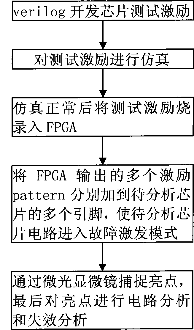
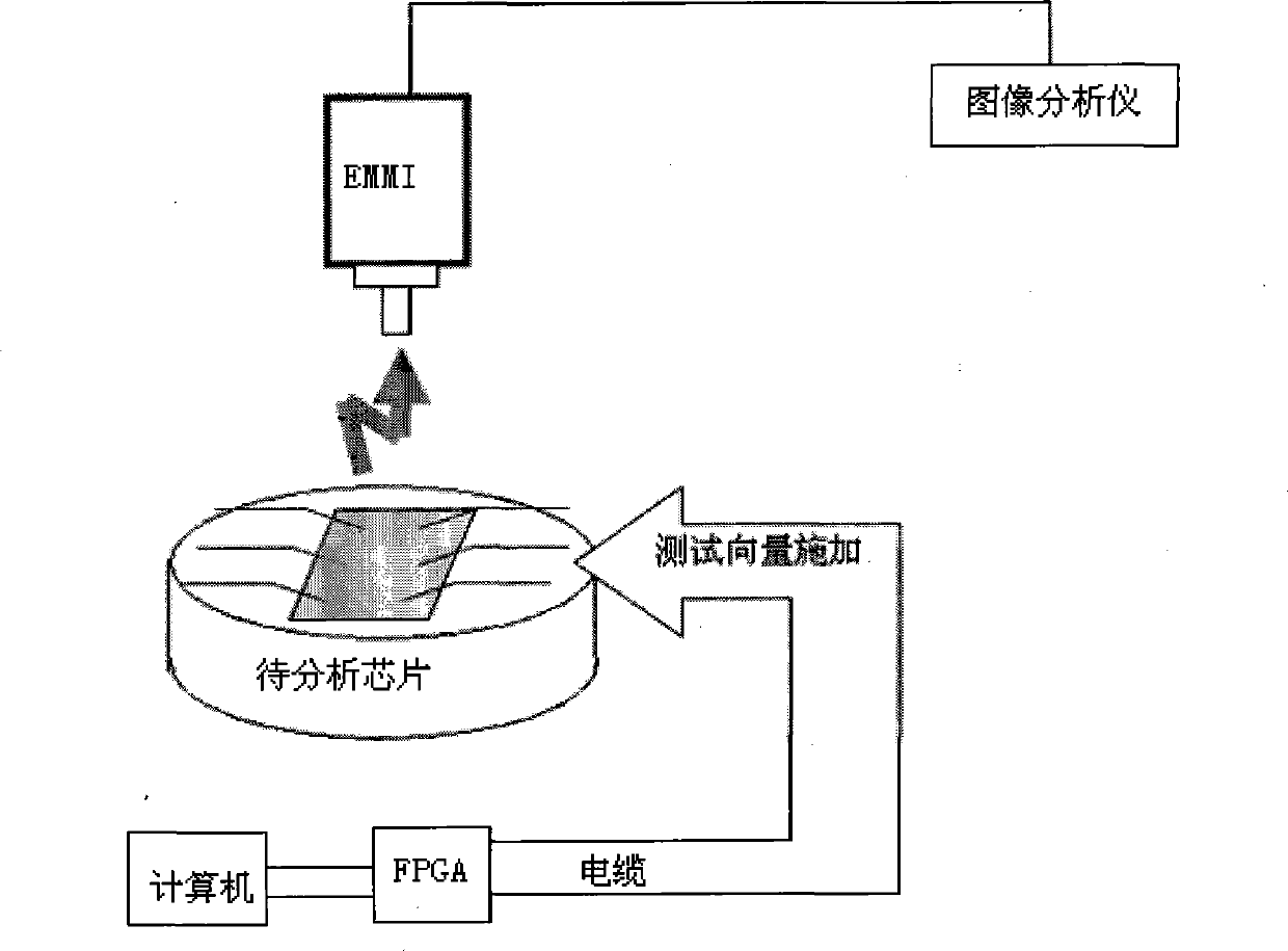
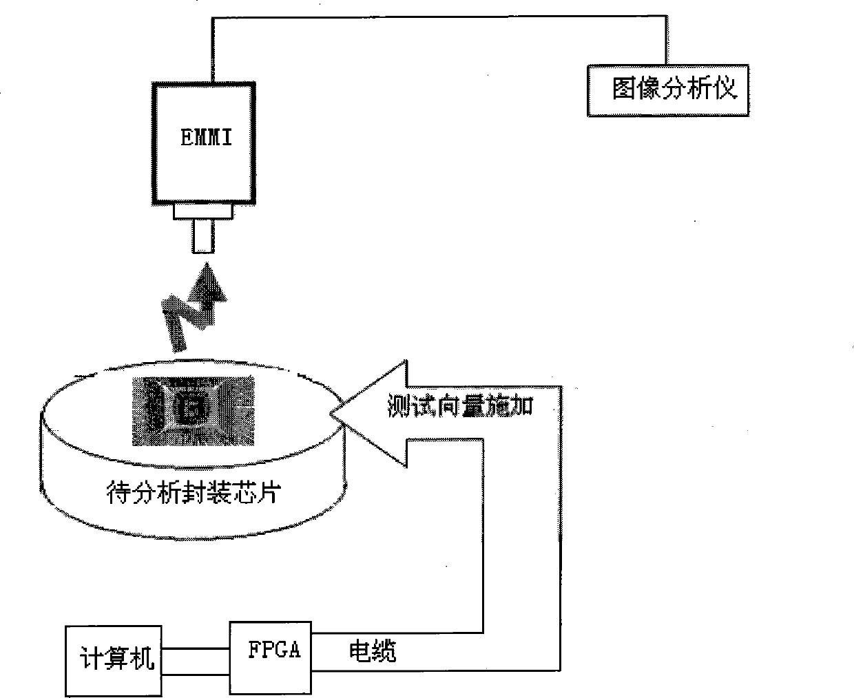
[0031] An embodiment of the micro-light microscope chip failure analysis method of the present invention is as follows: figure 1 shown, including the following steps:

[0032] 1. Using the hardware description language verilog to develop chip test incentives;

[0033] Two. use Quatus software to simulate the test stimulus, after the simulation is normal, the test stimulus is burned into the FPGA (Field Programmable Gate Array, Field Programmable Gate Array) substrate;

[0034] 3. The FPGA substrate has a plurality of excitation pattern outputs, and the plurality of excitation pattern outputs are respectively connected to a plurality of pins of the chip to be analyzed through cables, so that a plurality of excitation patterns are respectively added to a plurality of pins of the chip to be analyzed, Make the chip circuit to be analyzed enter the fault excitation mode;

[0035] 4. Capture the bright spots through the micro-light microscope (EMMI), and finally conduct circuit an...


PUM


Abstract

The invention discloses an emission microscope chip failure analyzing method. The method comprises the following steps of: developing chip test stimulus by utilizing a hardware description language; simulating the chip test stimulus by software, burning the chip test stimulus into an FPGA (Field Programmable Gate Array) substrate after the simulation becomes normal; outputting a plurality of stimulus pattern outputs to a plurality of pins of a chip to be analyzed by the FPGA substrate to ensure that the circuit of the chip to be analyzed enters a failure stimulus mode; and capturing a light-spot through the emission microscope, and performing circuit analysis and failure analysis on the light-spot. The invention also discloses an emission microscope chip failure analyzing system. By adopting the emission microscope chip failure analyzing method and system, multi-channel complex test vector application can be realized, a defect of the emission microscope chip can be positioned, the cost for chip failure analysis can be reduced, and the analyzing efficiency can be improved.

Description

technical field [0001] The invention relates to integrated circuit failure testing technology, in particular to a micro-light microscope chip failure analysis method and system. Background technique [0002] In a chip, electron-hole recombination emits photons. For example: when a bias voltage is applied to the pn junction, the electrons in the n region can easily diffuse to the p region, and the holes in the p region can also easily diffuse to the n region and then interact with the holes in the p region (or the electrons in the n region) Electron-hole recombination. For chip failure analysis, Emission Microscope (EMMI) is a very useful and highly efficient tool for chip failure analysis. The weak light emitted can detect the leakage current visible light caused by various component defects, and the corresponding fault types include ESD, Latch up, junction leakage, hotelectrons, oxide current leakage and so on. [0003] Using a low-light microscope for failure analysis o...

Claims


Application Information

Patent Timeline
Patent Type & Authority Patents(China)
IPC IPC(8): G01R31/311
Inventor 马香柏李强曾志敏
Owner SHANGHAI HUAHONG GRACE SEMICON MFG CORP
Why Eureka
Try Eureka