Method for fabricating an integrated circuit device

A technology for integrated circuits and components, which is applied in the field of the formation of integrated circuit components, can solve the problems of increasing the complexity of integrated circuit technology and production, and achieve the effects of reducing impact, reducing depth, and increasing reliability.

Active Publication Date: 2011-07-06
TAIWAN SEMICON MFG CO LTD
View PDF4 Cites 14 Cited by
  • Summary
  • Abstract
  • Description
  • Claims
  • Application Information

AI Technical Summary

Problems solved by technology

However, the above-mentioned progress will also increase the complexity of integrated circuit technology and production. In order to make the progress easy to understand, the development of integrated circuit technology requires similar production methods and development.

Method used


Image

  • Method for fabricating an integrated circuit device
  • Method for fabricating an integrated circuit device
  • Method for fabricating an integrated circuit device

Examples


Embodiment Construction

[0011] It is to be understood that the following disclosure provides various examples to illustrate various features of the invention. In order to simplify the description, specific embodiments, units, and combinations will be used for description. However, these specific examples are not intended to limit the present invention. For example, forming an element on another element includes the two elements being in direct contact, or the two elements being separated by other elements. In addition, in order to simplify the description, the present invention uses the same symbols in different drawings to indicate similar elements in different embodiments, but the above repeated symbols do not mean that the elements in different embodiments have the same corresponding relationship.

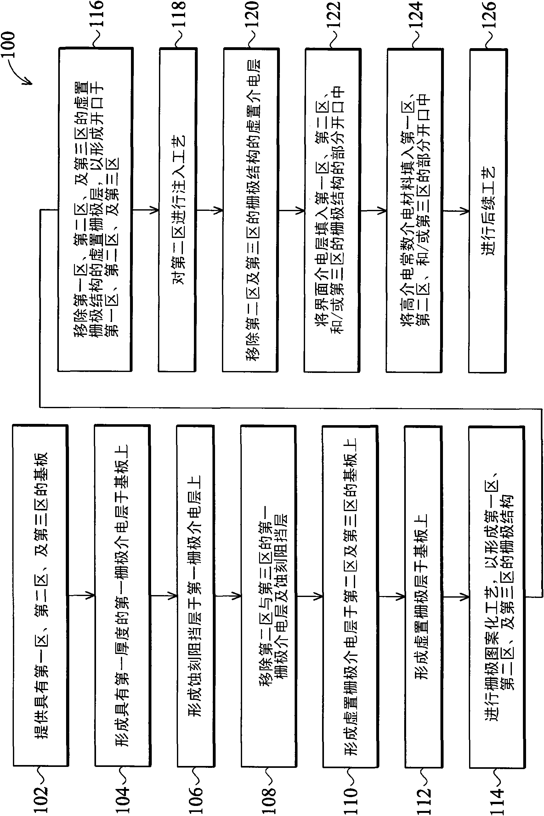
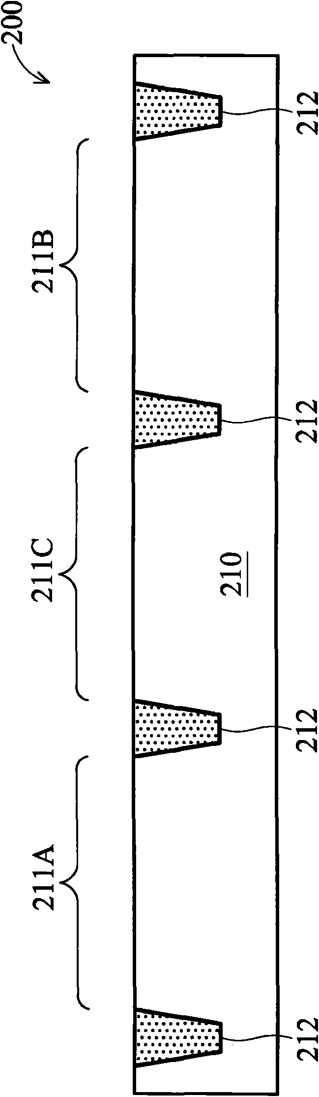
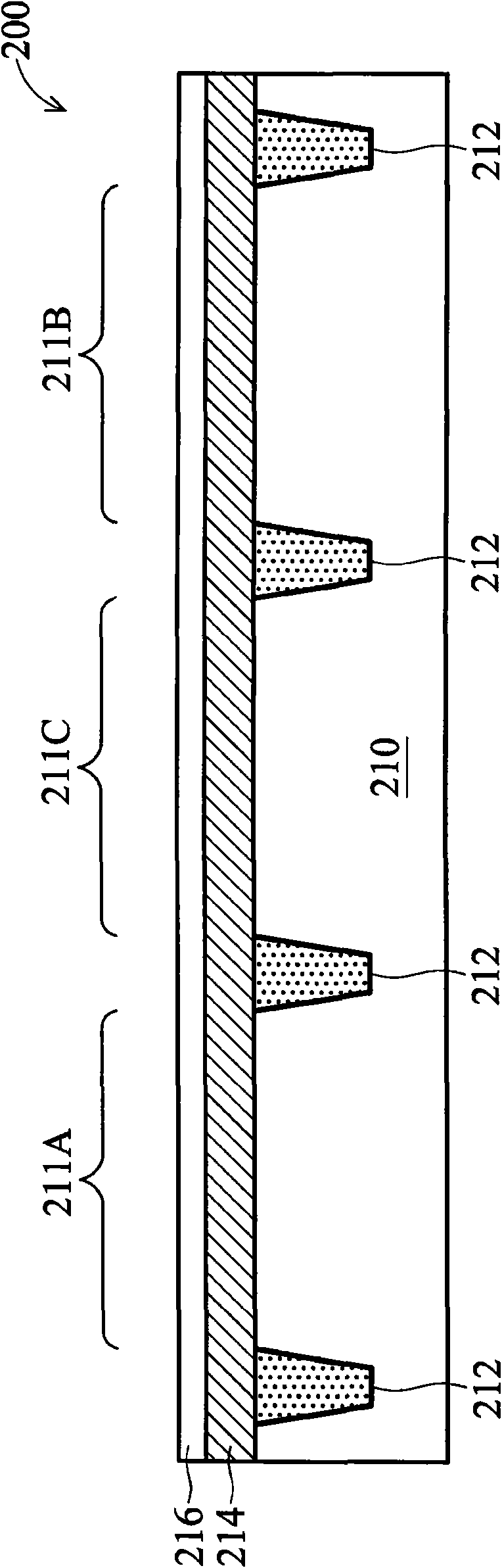
[0012] Next will be based on figure 1 Ways to 100 collocations Figure 2A-Figure 2K The semiconductor element 200 will be described. The semiconductor element 200 is a whole or part of an integrate...


PUM


Abstract

The present invention provides a method for fabricating an integrated circuit device. The method includes providing a substrate having a first region, a second region, and a third region; and forming a first gate structure in the first region, a second gate structure in the second region, and a third gate structure in the third region, wherein the first, second, and third gate structures include a gate dielectric layer, the gate dielectric layer being a first thickness in the first gate structure, a second thickness in the second gate structure, and a third thickness in the third gate structure. Forming the gate dielectric layer of the first, second, and third thicknesses can include forming an etching barrier layer over the gate dielectric layer in at least one of the first, second, or third regions while forming the first, second, and third gate structures, and / or prior to forming the gate dielectric layer in at least one of the first, second, or third regions, performing an implantation process on the at least one region. The method can reduce a number of etching oxidation layers of an active region.

Description

technical field [0001] The present invention relates to methods of forming integrated circuit components, and more particularly to forming integrated circuit components having gate dielectric layers of varying thicknesses. Background technique [0002] The semiconductor integrated circuit industry has grown rapidly for some time. In the process of integrated circuit progress, its functional density (the number of interconnected elements per unit area of ​​the chip) is getting larger and larger, while its size (the smallest element or connection that can be formed by the process) is getting smaller and smaller. . Process size reduction is beneficial for improving process efficiency and associated costs. However, the above-mentioned progress will also increase the complexity of integrated circuit technology and production. In order to make the progress easy to understand, the development of integrated circuit technology requires similar production methods and development. ...

Claims


Application Information

Patent Timeline
Patent Type & Authority Applications(China)
IPC IPC(8): H01L21/8234H01L21/28
CPCH01L29/665H01L29/7833H01L21/82345H01L21/823857H01L21/823842H01L29/66545H01L29/6659H01L21/823462H01L29/513
Inventor 许光源李达元李威养陶宏远
Owner TAIWAN SEMICON MFG CO LTD
Why Eureka
Try Eureka