Electrostatic discharge (ESD) protection structure of integrated circuit

An ESD protection and integrated circuit technology, applied in the direction of circuits, electrical components, electric solid devices, etc., can solve problems such as ineffective energy consumption, and achieve the effect of improving anti-ESD performance and high reliability

Inactive Publication Date: 2011-07-13
SUZHOU HUAXIN MICROELECTRONICS
View PDF4 Cites 1 Cited by
  • Summary
  • Abstract
  • Description
  • Claims
  • Application Information

AI Technical Summary

Problems solved by technology

d1 and d2 are set on the chip as a whole, so when the PN junction is reduced to a certain area, the melting of the intrinsic bulk silicon contained in it may not be able to effectively consume the energy generated when the ESD event occurs, thus causing an ESD event in the circuit happened

Method used


Image

  • Electrostatic discharge (ESD) protection structure of integrated circuit
  • Electrostatic discharge (ESD) protection structure of integrated circuit
  • Electrostatic discharge (ESD) protection structure of integrated circuit

Examples


Embodiment Construction

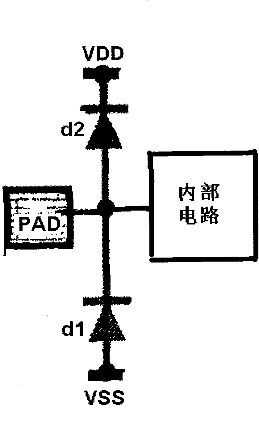
[0016] The ESD protection structure in the integrated circuit disclosed by the present invention is based on the prior art, and the prior art ( figure 1 In ), the PN junctions d1 and d2 formed as a whole are improved and designed, and they are designed as complex PN junctions placed between the internal circuit of the integrated circuit and the pad PAD without increasing the area occupied by the PN junction on the chip. These PN junctions form ESD protection for the internal circuits of integrated circuits in the form of semiconductor diodes.

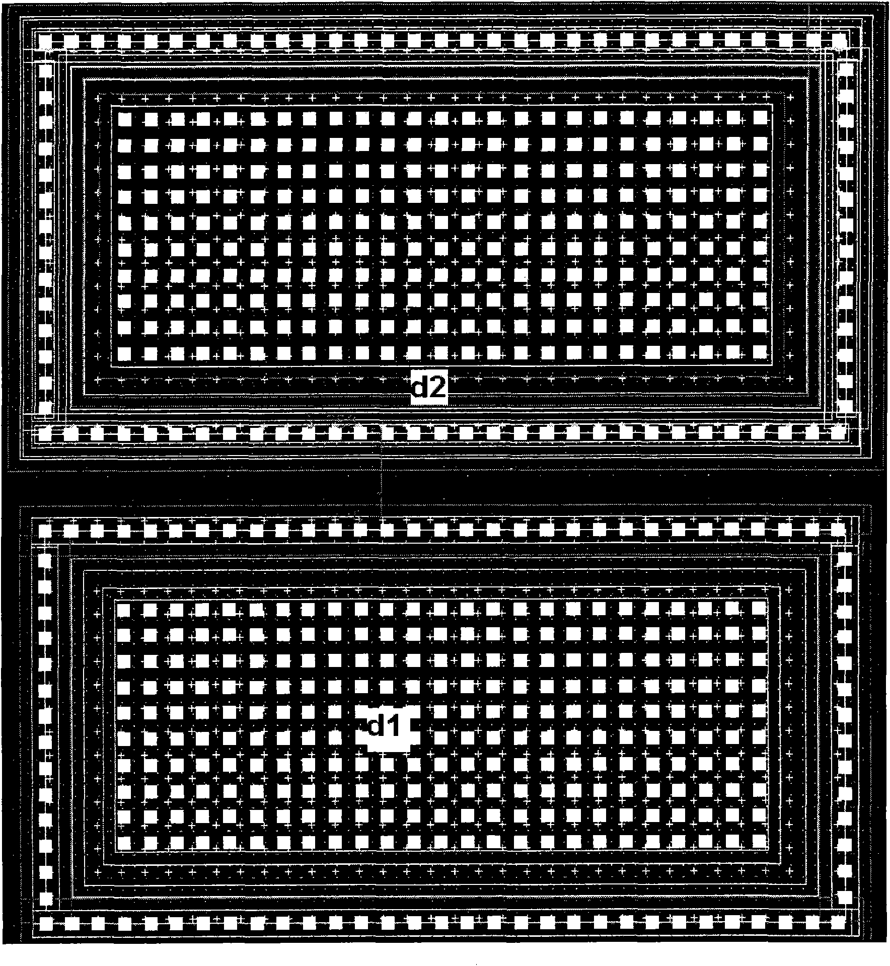
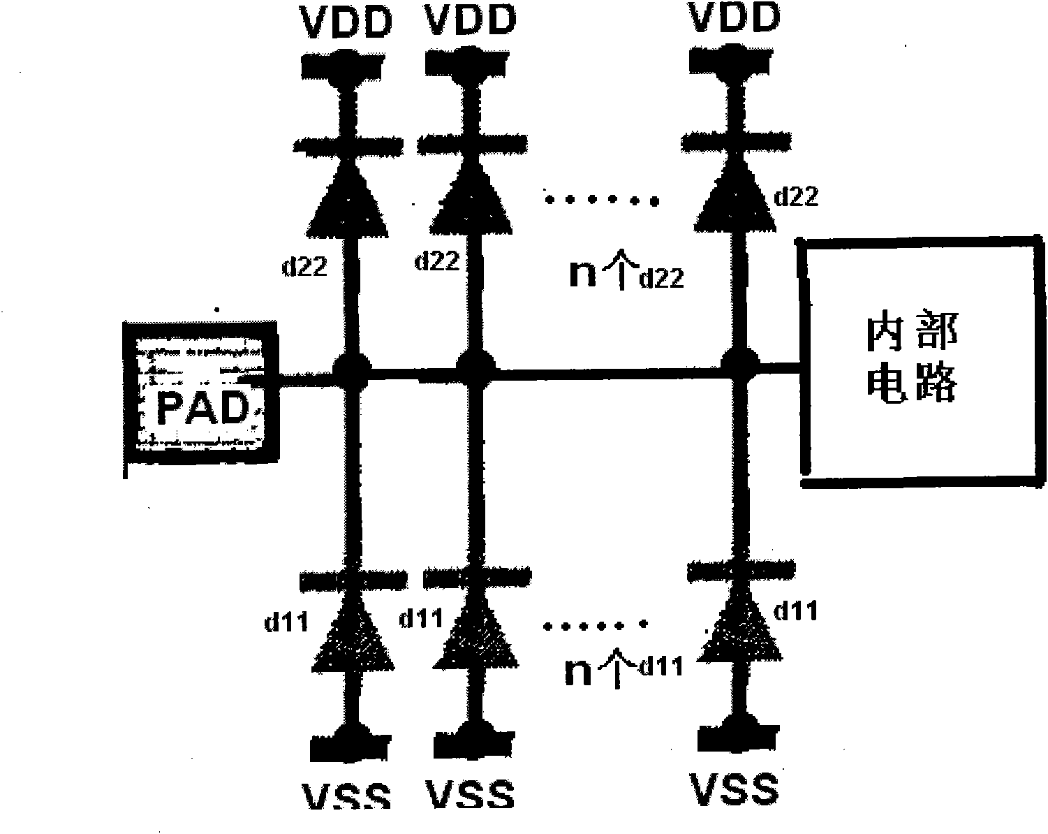
[0017] like image 3 As shown, the complex PN junctions of the ESD protection structure of the present invention include a plurality of first-type PN junctions d11 and a plurality of second-type PN junctions d22, wherein the plurality of first-type PN junctions d11 are connected in parallel, and It may be a PN junction such as NSD / PSUB type, and the plurality of second type PN junctions d22 are also connected in parallel, which may be ...


PUM


Abstract

The invention discloses an electrostatic discharge (ESD) protection structure of an integrated circuit. The ESD protection structure is arranged between an internal circuit and a bonding pad of the integrated circuit and consists of a PN junction which occupies a certain area of a chip of the integrated circuit, wherein the PN junction is set to be formed by parallelly connecting a plurality of small-area PN junctions on the occupied area of the chip, so that the volume of intrinsic silicon included in the PN junction is increased. In the novel ESD protection structure, the volume of the intrinsic silicon in a PN junction depletion region is increased without the increase of the occupied area on the chip, so that the influence of energy produced by an ESD event on a circuit can be more effectively reduced, and the ESD resistance of the circuit is improved.

Description

technical field [0001] The invention relates to the technical field of integrated circuits, in particular to an ESD protection structure of integrated circuits capable of improving the anti-ESD performance of circuits. Background technique [0002] As people's requirements for chips are getting higher and higher, in the application process of chips, people hope that not only the functions of chips are correct, but also the requirements for chip performance have been improved. An important factor affecting chip performance is ESD (Electrostatic Discharge, that is, electrostatic discharge). ESD will bring destructive consequences to the environment of electronic devices, and it is one of the main reasons for the failure of integrated circuits. With the continuous development of integrated circuit technology, the feature size of CMOS semiconductors continues to shrink, the gate oxide thickness of metal oxide semiconductors (MOS) is getting thinner and thinner, and the current a...

Claims


Application Information

Patent Timeline
Patent Type & Authority Applications(China)
IPC IPC(8): H01L27/02H01L23/60
Inventor 杭晓伟彭秋平张祯江石根谢卫国
Owner SUZHOU HUAXIN MICROELECTRONICS
Why Eureka
Try Eureka