Failure positioning method of chip

A failure location and chip technology, applied in the direction of electronic circuit testing, etc., can solve the problems of difficult operation and difficulty for users, and achieve the effect of improving accuracy, speed and speed

Inactive Publication Date: 2011-07-20
SUZHOU PIXCIR MICROELECTRONICS
View PDF4 Cites 10 Cited by
  • Summary
  • Abstract
  • Description
  • Claims
  • Application Information

AI Technical Summary

Problems solved by technology

In actual operation, if many probes work at the same time, it is difficult for users to operate
For example, when four signal inputs are required, plus the power signal and ground signal of the chip itself, a total of six probe heads are requi

Method used


Image

  • Failure positioning method of chip
  • Failure positioning method of chip
  • Failure positioning method of chip

Examples


Example Embodiment

[0010] The present invention will be further described below in conjunction with the accompanying drawings and embodiments.

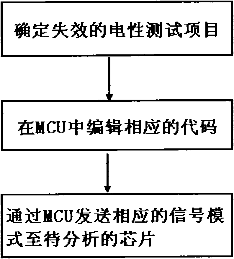
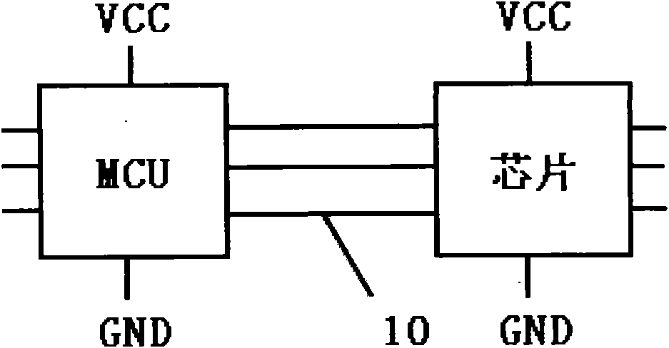
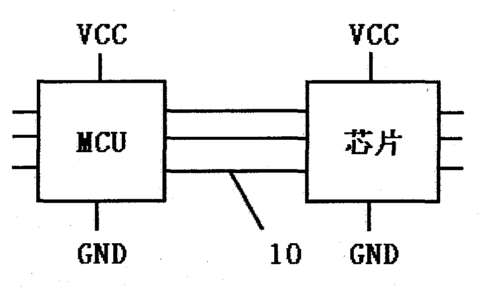
[0011] The so-called failure location of the chip refers to observing the hot spots of the normal chip and the failed chip under the Emmision Microscope (EMMI for short), finding the abnormal points through comparison, and further analyzing the root cause of the chip failure. Therefore, when performing failure analysis on the chip, it is first necessary to determine the failed electrical test items. Since many items on the chip can be tested, such as whether the pins on the chip are leaking, static power consumption, and dynamic power consumption, etc., so when performing Test items need to be specified before failure location. The chip itself contains several modules, and different modules control different functions on the chip. Therefore, when the signal at the input end is the same, the chip module after failure is different from the normal module....


PUM


Abstract

The invention relates to a failure positioning method of a chip, comprising the following steps of: ensuring a failure electric testing item; then editing corresponding codes in an MCU (Microprogrammed Control Unit); and finally, sending a corresponding signal mode to the to-be-analyzed chip via the MCU. The failure positioning method of the chip is simple and faster in speed; the accuracy and the speed are greatly improved when operation; as the MCU is used as a signal generator, the MCU can send any needed signals and can simulate each state of the chip during working, thereby testing any failure item of the chip.

Description

technical field [0001] The invention relates to the technical field of chip failure analysis, in particular to a method for chip failure location. Background technique [0002] Due to the inevitable failure of integrated circuits in the process of development, production and use, and with the continuous improvement of people's requirements for product quality and reliability, failure analysis is becoming more and more important. Through chip failure analysis, it can help integrated circuit designers To find design defects, mismatch of process parameters, or improper design and operation, so the significance of failure analysis is particularly important. First of all, failure analysis is a necessary means to determine the failure mechanism of the chip; secondly, failure analysis provides the necessary information for effective fault diagnosis; then, failure analysis is for design engineers to continuously improve or repair the design of the chip to make it more consistent wit...

Claims


Application Information

Patent Timeline
IPC IPC(8): G01R31/28
Inventor 叶本银
Owner SUZHOU PIXCIR MICROELECTRONICS
Why Eureka
Try Eureka