
Semiconductor packaging process and die utilized in same

A packaging process and semiconductor technology, which is applied in the fields of semiconductor devices, semiconductor/solid-state device manufacturing, and electrical solid-state devices, and can solve problems such as reducing yield and increasing efficiency and cost.

Active Publication Date: 2011-07-20
ADVANCED SEMICON ENG INC
View PDF0 Cites 3 Cited by
  • Summary
  • Abstract
  • Description
  • Claims
  • Application Information

AI Technical Summary

Problems solved by technology

Therefore, before clamping the other half of the finished product, the mold 1 must be cleaned first, thereby reducing efficiency and increasing costs, otherwise, the adhesive 22 will stick to the other half of the finished product, thereby reducing the yield

Method used


Image

  • Semiconductor packaging process and die utilized in same
  • Semiconductor packaging process and die utilized in same
  • Semiconductor packaging process and die utilized in same

Examples


Embodiment Construction

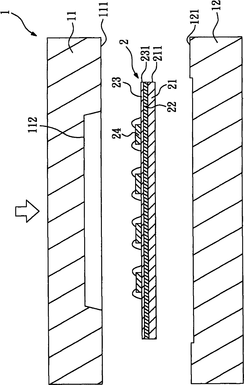
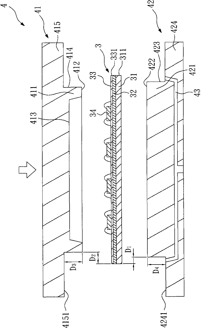
[0012] refer to Figure 3 to Figure 5 , showing a schematic diagram of the semiconductor packaging process of the present invention. refer to image 3 , provide a half finished product 3 and a mold 4 . The semi-finished product 3 includes a carrier 31 , an adhesive 32 , a semiconductor substrate 33 and at least one semiconductor component 34 , and the carrier 31 has a first outer peripheral surface 311 . The semiconductor substrate 33 is a wafer or an interposer, which has a second peripheral surface 331 , and is adhered to the carrier 31 by the adhesive 32 , so that the carrier 31 serves as a support for the semiconductor substrate 33 . The semiconductor component 34 is disposed on the semiconductor substrate 33 . The mold 4 includes an upper mold 41 and a lower mold 42, the upper mold 41 has a pressing portion 411, the pressing portion 411 has a pressing surface 412, at least one mold cavity 413 and a third outer peripheral surface 414, the The mold cavity 413 is opened ...


PUM


Abstract

The invention relates to a semiconductor packaging process and a die utilized in same. The die is used for clamping a semi-finished product and comprises an upper die and a lower die. The upper die comprises a first base and a pressing part, wherein the pressing part is protruded on the first base and comprises a pressing surface and at least one die cavity. The lower die comprises a second base and a bearing part, wherein the bearing part is protrusive on the second base and comprises a bearing surface. Therefore, when the semiconductor packaging process is performed, viscose in the semi-finished product can be prevented from being sticked to the die, thereby improving the yield, improving the efficiency and reducing the cost.

Description

technical field [0001] The present invention relates to a semiconductor packaging process and a mold used in the semiconductor packaging process, in detail, to a semiconductor packaging process that avoids sticking of glue and a mold used in the semiconductor packaging process. Background technique [0002] refer to figure 1 , shows a schematic cross-sectional view of a known die used in semiconductor packaging processes. The known mold 1 used in the semiconductor packaging process is used to hold a semi-finished product 2 and includes an upper mold 11 and a lower mold 12 . The upper mold 11 has a pressing surface 111 and at least one mold cavity 112 , and the mold cavity 112 is opened on the pressing surface 111 . The lower mold 12 has a bearing surface 121 . The semi-finished product 2 includes a carrier 21 , an adhesive 22 , a semiconductor substrate 23 and at least one chip 24 . The carrier 21 has a first peripheral surface 211 , the semiconductor substrate 23 has a ...

Claims


Application Information

Patent Timeline
Patent Type & Authority Applications(China)
IPC IPC(8): H01L21/50H01L21/56
CPCH01L2224/48091H01L2224/48227H01L2924/181H01L2924/00014H01L2924/00012
Inventor 彭胜扬
Owner ADVANCED SEMICON ENG INC
Learn More