Multi-project wafer cutting method supporting constraint and limitation on positions of chips

A technology that supports chips and dicing methods, applied in semiconductor/solid-state device manufacturing, electrical components, circuits, etc., can solve problems such as chip combination, difficulty in achieving mask area, and inability to minimize mask area, so as to achieve cost reduction Effect

Active Publication Date: 2011-07-20
SEMITRONIX
View PDF3 Cites 7 Cited by
  • Summary
  • Abstract
  • Description
  • Claims
  • Application Information

AI Technical Summary

Problems solved by technology

Therefore, the traditional chip automatic layout planning technology does not support this function, and thus cannot achieve the purpose of minimizing the area of ​​the mask plate formed by chip arrangement and combination; It is more difficult to achieve the requirement of minimizing the mask area as much as possible under the condition that the chip is limited by the position constraints.

Method used


Image

  • Multi-project wafer cutting method supporting constraint and limitation on positions of chips
  • Multi-project wafer cutting method supporting constraint and limitation on positions of chips
  • Multi-project wafer cutting method supporting constraint and limitation on positions of chips

Examples


Embodiment Construction

[0069] In order to describe the present invention more specifically, the multi-item wafer cutting method of the present invention will be described in detail below in conjunction with the accompanying drawings and specific embodiments.

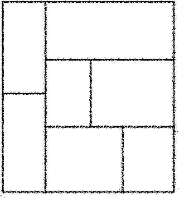
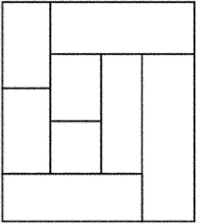
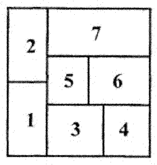
[0070] Such as Figure 6As shown, the flow of a multi-item wafer dicing method that supports chip position constraints is as follows:

[0071] (1) Obtain information on the number, area and location of chips;

[0072] The position placement information includes the information of placing some chips at specific positions on the mask according to the actual production test requirements and the information of placing some chips with the same or similar shape and size at adjacent positions, and any of the two chips If the side lengths are equal, the two shapes are considered to be similar in size.

[0073] (2) According to the placement information of chips in step (1), the chips with the same or similar shape and size that need to be placed in ...


PUM


Abstract

The invention discloses a multi-project wafer cutting method supporting constraint and limitation on the positions of chips, and the method comprises the following steps: performing relative and absolute position constraint on a mask plate against the chips according to actual production and testing requirements; re-adjusting and defining a general objective equation of a simulated annealing algorithm in the layout planning method; and simultaneously enabling the chips which are in the same or similar size and need to be placed in the adjacent positions to attribute to a same layout group, thereby ensuring that the chips or sub-layout groups in the same layout group to be always positioned in the adjacent positions, effectively reducing the iteration number and the time of the simulated annealing algorithm, realizing automation of layout planning of the chips under the constraint and the limitation in the specific positions, further greatly reducing the area of the mask plate, dividing more mask plates on one wafer by cutting, and greatly reducing the corresponding cost.

Description

technical field [0001] The invention relates to a wafer cutting method, in particular to a multi-item wafer cutting method that supports chip positions being restricted. Background technique [0002] Multi Project Wafer (Multi Project Wafer, referred to as MPW), is to put a variety of integrated circuit designs with the same process on the same mask (Reticle / Mask, also known as reticle). After the manufacturing is completed, each Dozens of chip samples can be obtained for a design project, which is enough for experiments and tests in the prototype (Prototype) design stage. The manufacturing cost is shared by all the projects participating in the multi-project wafer according to their respective chip areas, and the cost is only 5%-10% of the cost of prototype manufacturing for a single project, which greatly reduces product development risks. The threshold for cultivating integrated circuit design talents and the threshold for small and medium integrated circuit design compa...

Claims


Application Information

Patent Timeline
Patent Type & Authority Applications(China)
IPC IPC(8): H01L21/78H01L21/00
Inventor 叶翼张波任杰郑勇军马铁中
Owner SEMITRONIX
Why Eureka
Try Eureka