Composite electrode of light-emitting diode chip and manufacturing methods thereof

A technology of light-emitting diodes and composite electrodes, which is applied in the direction of circuits, electrical components, semiconductor devices, etc., can solve the problems of high cost, complicated electrode production process, and difficult storage of products, and achieve the effects of cost reduction and strong environmental adaptability

Inactive Publication Date: 2011-07-20
DALIAN MEIMING EPITAXIAL WAFER TECH
View PDF3 Cites 40 Cited by
  • Summary
  • Abstract
  • Description
  • Claims
  • Application Information

AI Technical Summary

Problems solved by technology

[0006] In order to solve the above-mentioned problems such as complex production process of light-emitting diode chip electrodes, high cost, and difficult preservation of products, the present invention proposes a composite electrode of light-emitting diode chips and its manufacturing method

Method used


Image

  • Composite electrode of light-emitting diode chip and manufacturing methods thereof
  • Composite electrode of light-emitting diode chip and manufacturing methods thereof
  • Composite electrode of light-emitting diode chip and manufacturing methods thereof

Examples


Embodiment 1

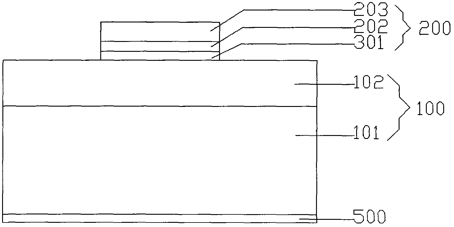
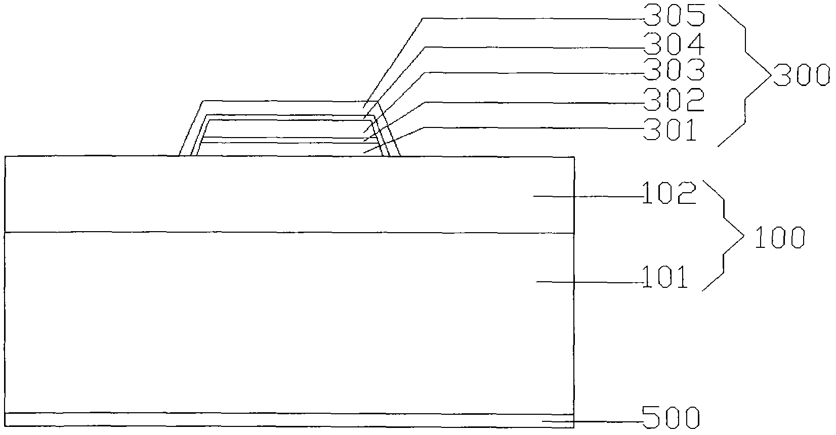
[0076] A compound electrode (300) of a light-emitting diode chip, the structure of which is respectively from bottom to top: an ohmic contact metal layer (301), a first isolation metal layer (302), a filling metal layer (303), and a second isolation metal layer (304), the surface metal layer (305), wherein the second isolation metal layer (304) and the surface metal layer (305) cover the ohmic contact metal layer (301), the first isolation metal layer (302) and the filling metal layer The top and side of (303) completely wrap these three electrode layers inside the electrode, such as figure 2 . Wherein, the ohmic contact metal layer (301) is an AuBe alloy with a thickness of 10nm; the first isolation metal layer (302) is Ti with a thickness of 5nm; the filling metal layer (303) Al is 100nm; the second isolation metal layer (304 ) is Ti with a thickness of 5nm; the surface metal layer (305) is Au with a thickness of 50nm.

[0077] The manufacturing method of the composite el...

Embodiment 2

[0092] A composite electrode (300) for a light emitting diode chip, the structure of which is the same as that in Embodiment 1.

[0093] The difference from Example 1 is that the method for making the composite electrode (300) of the LED chip includes the following steps:

[0094] a) providing a piece of LED epitaxial wafer (100);

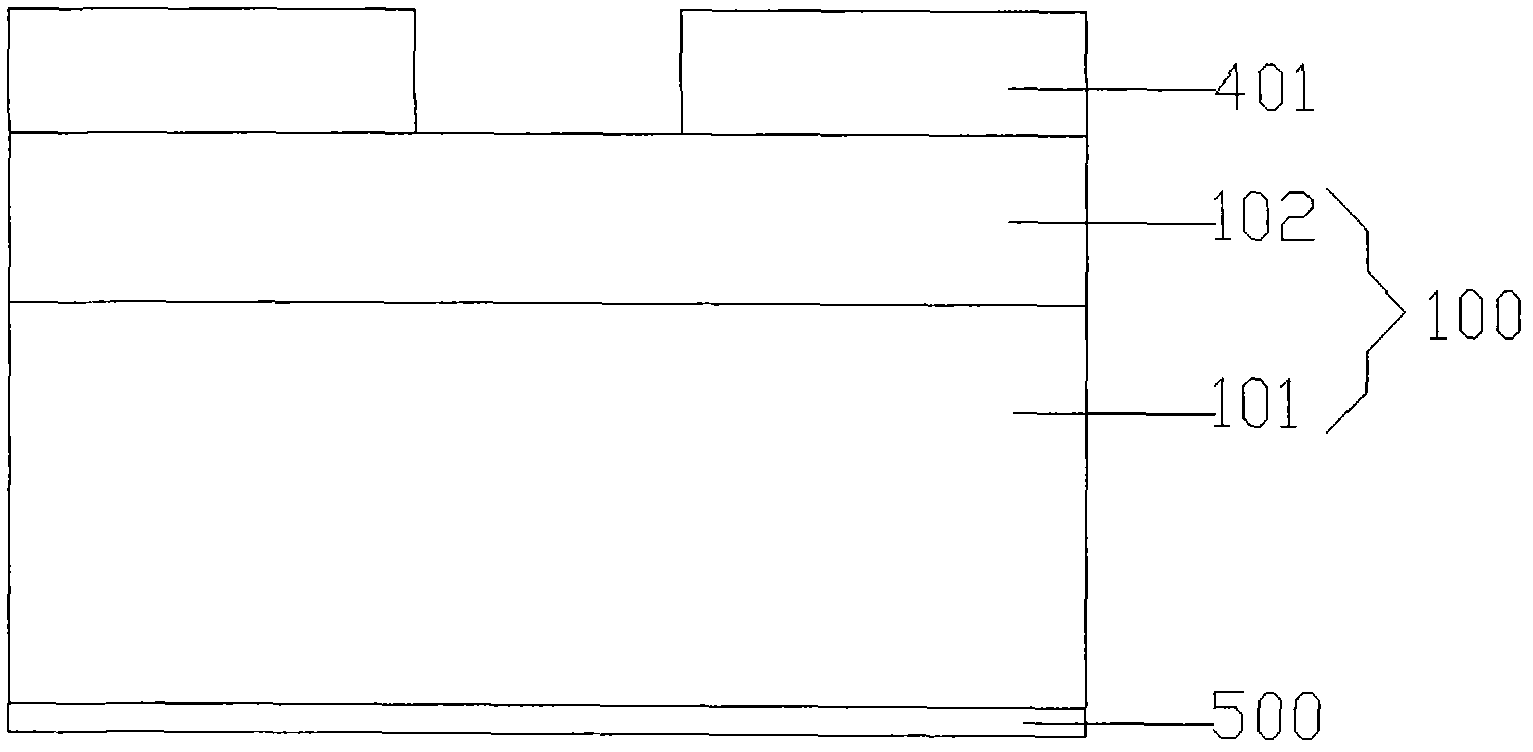
[0095] b) Fabricate the first covering layer (401) and the second covering layer (402) sequentially from bottom to top on the upper surface of the light-emitting epitaxial layer (102) of the LED epitaxial wafer (100), such as Figure 8 ;

[0096] c) exposing the second cover layer (402) to make electrode patterns;

[0097] d) Perform wet etching on the exposed epitaxial wafer, etch and remove the second covering layer (402) and the first covering layer (401) at the electrode pattern to form an inverted funnel-shaped hollow area, exposing the light-emitting epitaxial layer below The upper surface of (102), such as Figure 9 ;

[0098] e) Use ev...

Embodiment 3

[0106] A compound electrode (300) of a light-emitting diode chip, its structure is different from Embodiment 1 in that: its ohmic contact metal layer (301) is Ti and Zn, the thickness is 300nm, and the first isolation metal layer (302) is W , its thickness is 50nm; The filling metal layer (303) is Ag, and its thickness is 1000nm; The second isolation metal layer (304) is Pt, and its thickness is 50nm; Surface metal layer (305) is Au, and its thickness is 200nm.

[0107] The fabrication method of the composite electrode (300) is the same as that in Example 1, except that the thickness of the first covering layer (401) is 2000 nm.


PUM

PropertyMeasurementUnit
thicknessaaaaaaaaaa
thicknessaaaaaaaaaa
thicknessaaaaaaaaaa

Abstract

The invention belongs to the field of light-emitting semiconductors, and particularly relates to the field of light-emitting diode chips. The structure of a composite electrode of the light-emitting diode chip comprises an ohmic contact metal layer, a first isolated metal layer, a filled metal layer, a second isolated metal layer and a surface metal layer from bottom to top respectively, wherein the second isolated metal layer and the surface metal layer are covered on the upper surfaces and the side surfaces of the ohmic contact metal layer, the first isolated metal layer and the filled metal layer so as to completely wrap the three electrode layers in the electrode. The invention further comprises two manufacturing methods of the composite electrode, which are the method I and the method II respectively. The composite electrode uses Al, Ag and other active metals with low using cost to replace part of Au in the electrode, thereby reducing the cost of the electrode and having stronger ability to adapt to the environment; through multiple tests by an author, the composite electrode can be quickly effectively manufactured by the two methods, the manufacturing process is simple and feasible, the operability is high, and the large-scale production is convenient.

Description

technical field [0001] The invention belongs to the field of light-emitting semiconductors, especially the field of light-emitting diode chips. Background technique [0002] A semiconductor light-emitting diode is a photoelectric element made of semiconductor materials. It is a solid-state light source that can directly convert electrical energy into light energy. Semiconductor light-emitting diodes have the advantages of high reliability, high efficiency, long life, full solidification, low power consumption, and quick response. They have a huge application market in the fields of large-screen display, traffic information indicator, general optical display and indication. [0003] Conventional light-emitting diode (LED) structures such as figure 1 As shown, it includes two types of front electrode (200) and back electrode (500), wherein the thickness of the front electrode (200) is between 1.5 microns and 2 microns, mostly Au electrodes, including ohmic contact metal layer...

Claims


Application Information

Patent Timeline
Patent Type & Authority Applications(China)
IPC IPC(8): H01L33/36H01L33/40H01L33/00
Inventor 肖志国常远王力明武胜利高本良康建
Owner DALIAN MEIMING EPITAXIAL WAFER TECH
Why Eureka
Try Eureka