Open-circuit embedding-removing test structure for trimmer-capacitance MOS (metal oxide semiconductor) varactor and variable capacitance diode

A varactor diode, open circuit de-embedding technology, applied in circuits, electrical components, electrical solid devices, etc., can solve the problem of inability to completely remove parasitic capacitance, and achieve the effect of improving consistency

Active Publication Date: 2011-07-27
SEMICON MFG INT (SHANGHAI) CORP +1
View PDF0 Cites 9 Cited by
  • Summary
  • Abstract
  • Description
  • Claims
  • Application Information

AI Technical Summary

Problems solved by technology

[0013] In order to solve the problem that the open-circuit de-embedding test structure of the micro-capacitance MOS varactor and varactor diode cannot completely remove the parasitic capacitance, and improve the consistency between the parameters of the open-circuit test structure and the actual circuit parameters, the present invention provides a microcapacitance MOS The open-circuit de-embedding test structure of the varactor and the varactor diode, the open-circuit de-embedding test structure includes: a plurality of metal layers and an active area; the plurality of metal layers includes a top metal layer, connected to the active area The first metal layer and at least one intermediate metal layer between the top metal layer and the first metal layer, the first metal layer includes a loop; the top metal layer is divided into four disconnected area, the area includes: two signal port top metal layer areas respectively connected to two signal ports, and two adjacent ground ports on the same side of the two signal port connection directions are respectively connected together Two ground port top metal

Method used


Image

  • Open-circuit embedding-removing test structure for trimmer-capacitance MOS (metal oxide semiconductor) varactor and variable capacitance diode
  • Open-circuit embedding-removing test structure for trimmer-capacitance MOS (metal oxide semiconductor) varactor and variable capacitance diode
  • Open-circuit embedding-removing test structure for trimmer-capacitance MOS (metal oxide semiconductor) varactor and variable capacitance diode

Examples


Example Embodiment

[0034] In the following description, a lot of specific details are given in order to provide a more thorough understanding of the present invention. However, it is obvious to those skilled in the art that the present invention can be implemented without one or more of these details. In other examples, in order to avoid confusion with the present invention, some technical features known in the art are not described.

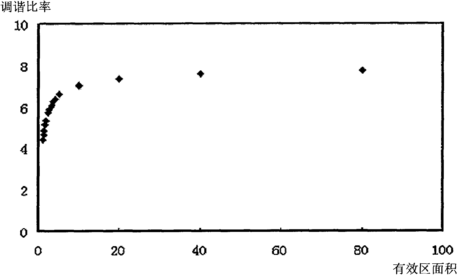
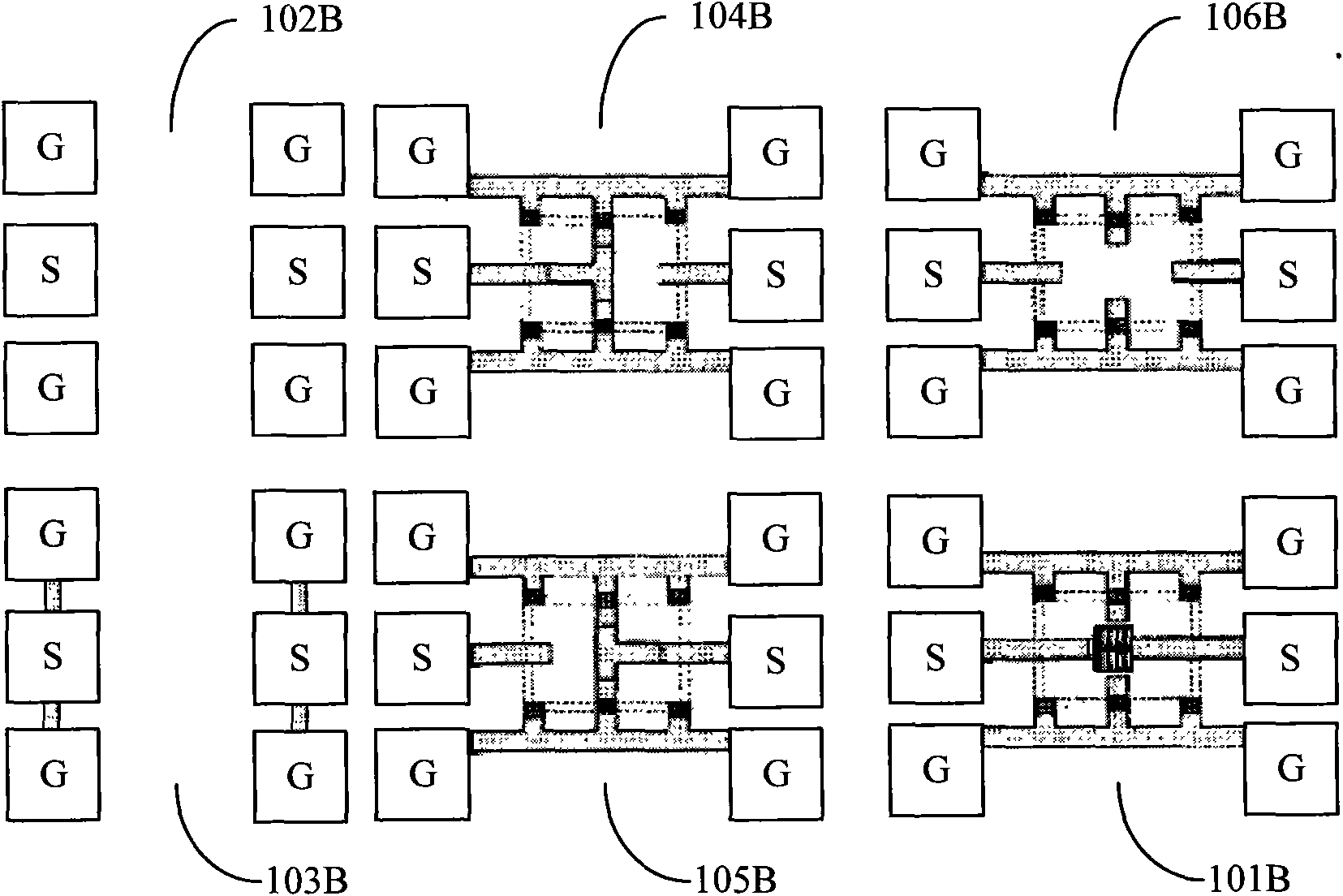
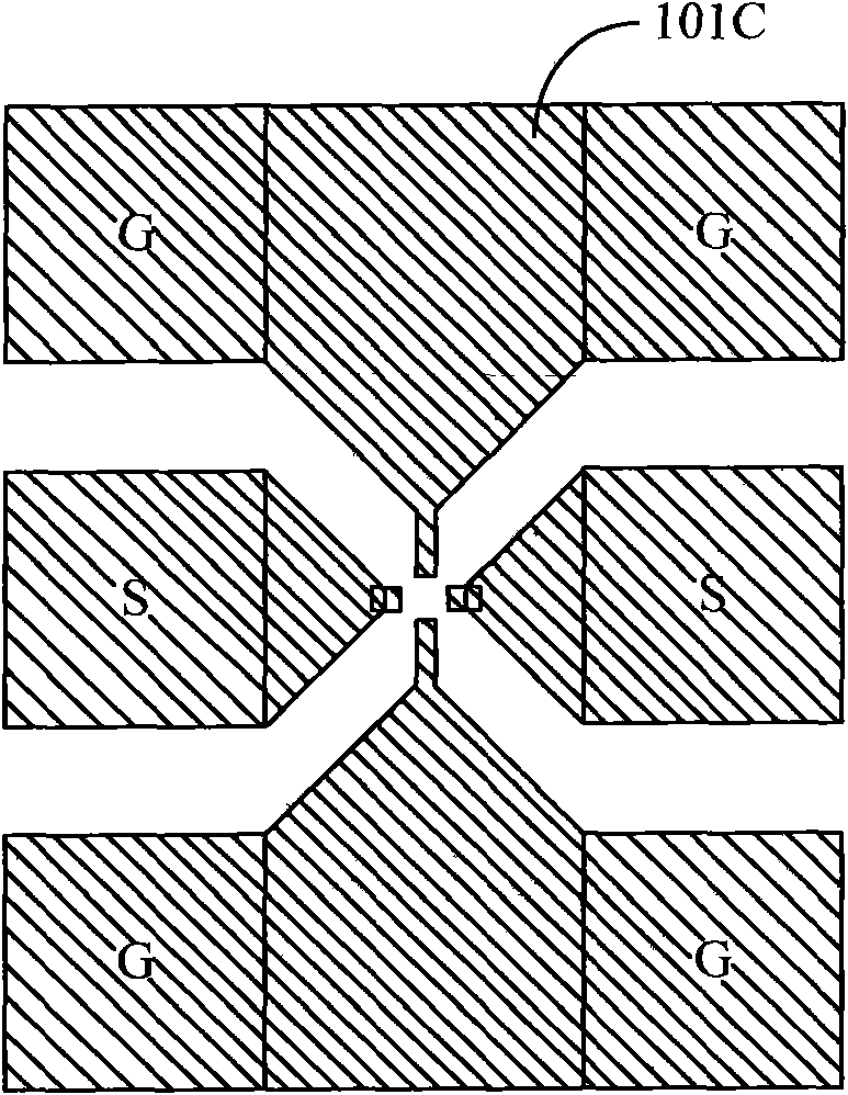
[0035] In order to thoroughly understand the present invention, a detailed structure will be presented in the following description to illustrate how the present invention solves the problem that the open circuit de-embedding test structure of the microcapacitor MOS varactor and varactor diode cannot completely eliminate the parasitic capacitance. Obviously, the implementation of the present invention is not limited to the specific details familiar to those skilled in the semiconductor field. The preferred embodiments of the present invention are described in detail...


PUM


Abstract

The invention discloses an open-circuit embedding-removing test structure for a trimmer-capacitance MOS (metal oxide semiconductor) varactor and a variable capacitance diode, which comprises a plurality of metal layers and an active area; the plurality of metal layers comprise a top metal layer, a first metal layer connected with the active area, and at least one middle metal layer between the top metal layer and the first metal layer; the first metal layer comprises a loop; the top metal layer is divided into four unconnected port top metal layer areas; the scopes of the areas of the middle metal layer below each area are all in the scopes of the corresponding port top metal layer areas; an earthing port top metal layer area is connected with the middle metal layer area below thereof andthe loop of the first metal layer one by one; and at least one layer of middle metal area below a signal port top metal layer area is removed to cut off the connection between the signal port top metal layer area and the first metal layer. The open-circuit embedding-removing test structure can effectively eliminate parasitic capacitances, and improve the consistency between the parameters of the test structure and the actual circuit parameters.

Description

technical field [0001] The invention relates to the technical field of semiconductors, in particular to an open-circuit de-embedding test structure of a microcapacitance MOS varactor and a varactor. Background technique [0002] Metal oxide semiconductor (MetalOxide Semiconductor, hereinafter referred to as: MOS) varactors and varactor diodes are components whose capacitance varies with voltage, and are radio frequency and mixed signal (mix-signal) circuits, especially voltage controlled oscillators (Voltage Controlled Oscillator, hereinafter referred to as: VCO) is an important component in the circuit. With the development of integrated circuits, the driving frequency of some circuits has exceeded 3GHz. For example, in high-speed circuits, the VCO circuit that generates the clock signal needs to use a minimum capacitance value less than or equal to 100fF (10 -10 F) microcapacitance MOS varactor or varactor diode. [0003] In order to obtain various parameters of the circ...

Claims


Application Information

Patent Timeline
IPC IPC(8): H01L23/58H01L29/93H01L29/94
Inventor 蒋立飞吴颜明
Owner SEMICON MFG INT (SHANGHAI) CORP
Why Eureka
Try Eureka