Method for forming electrical interconnection in organic optoelectronic device, method for making organic optoelectronic device and organic optoelectronic device
A technology for organic electronic devices and electrical interconnection, which is used in the manufacture of semiconductor/solid-state devices, electric solid-state devices, photovoltaic power generation, etc., to achieve the effects of uniformity improvement, process simplification, and series resistance improvement.
- Summary
- Abstract
- Description
- Claims
- Application Information
AI Technical Summary
Problems solved by technology
Method used
Image

Examples
example 1
[0152] Example 1): Organic Light Emitting Devices Including Electrical Interconnects
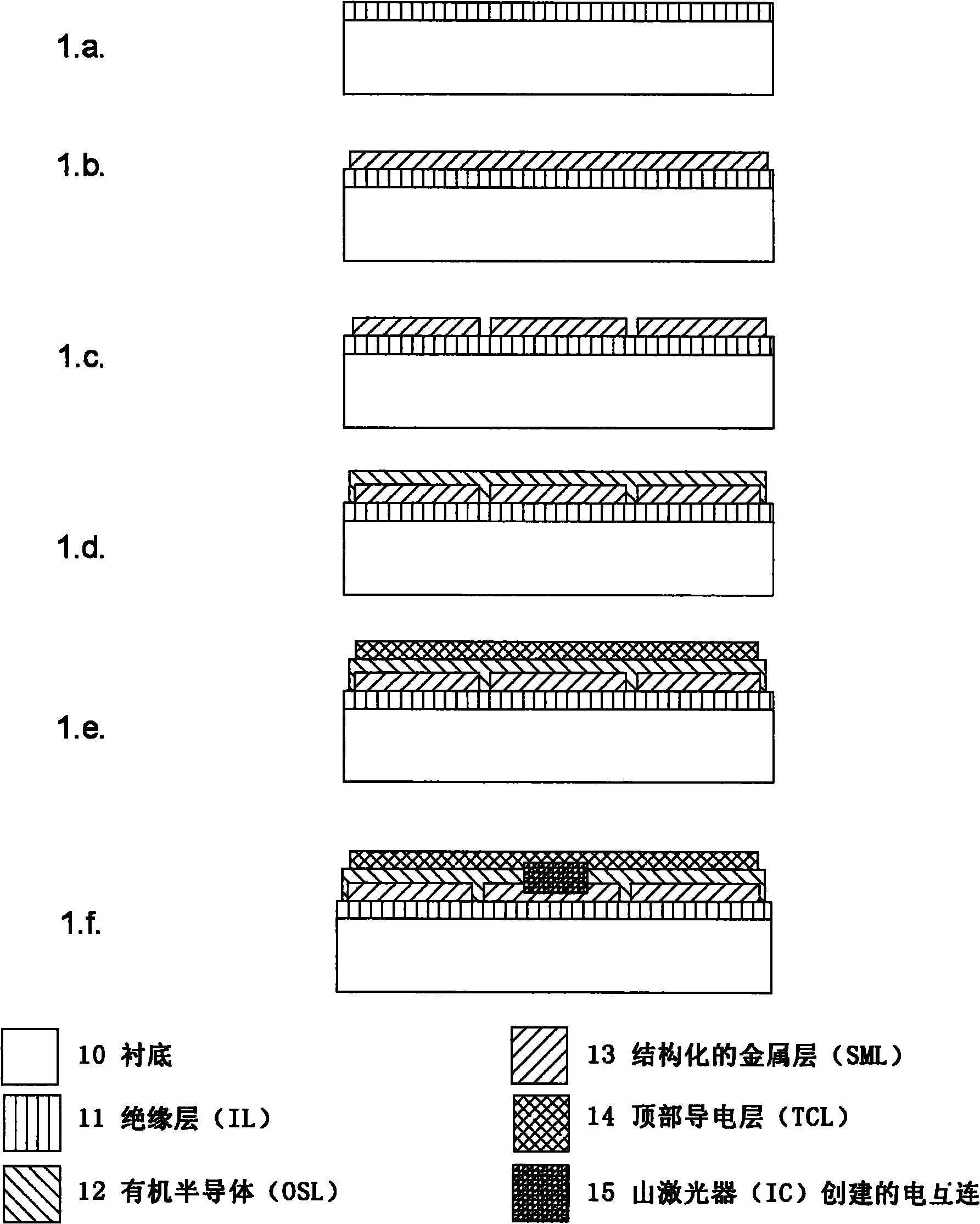
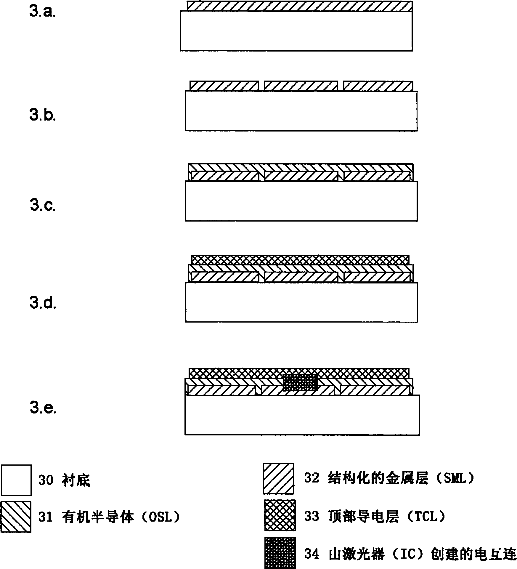
[0153] Provide 100mm×100mm glass substrate. A 90 mm x 78 mm metal layer SML is deposited on the glass substrate. The metal layer is patterned to form parallel strips: a wide strip (RA-area A) with dimensions 90mm x 20mm and a narrow strip (RB-area B) with dimensions 90mm x 3mm; between the strips There is always a 1mm space. Stripes were formed in the following configuration: (RB)-3 x ((RA)-(RB)) ("-" indicates lateral layer separation). This configuration is compatible with Figure 4 SML in is similar.
[0154] An unpatterned 80 mm x 78 mm OSL comprising the following layers was deposited on the SML as follows: 50 nm thick NPD layer doped with F4TCNQ; 10 nm thick undoped NPD layer; 20 nm blue emitter main layer doped with fluorescent emitters 10 nm of BPhen; 60 nm of BPhen doped with Cs. And, a 20 nm Ag layer was deposited as TCL.
[0155] The overlap between OSL, (RA) and TCL form...
example 2
[0158] Example 2): Organic Light Emitting Devices and Electrical Interconnects on Metal Substrates
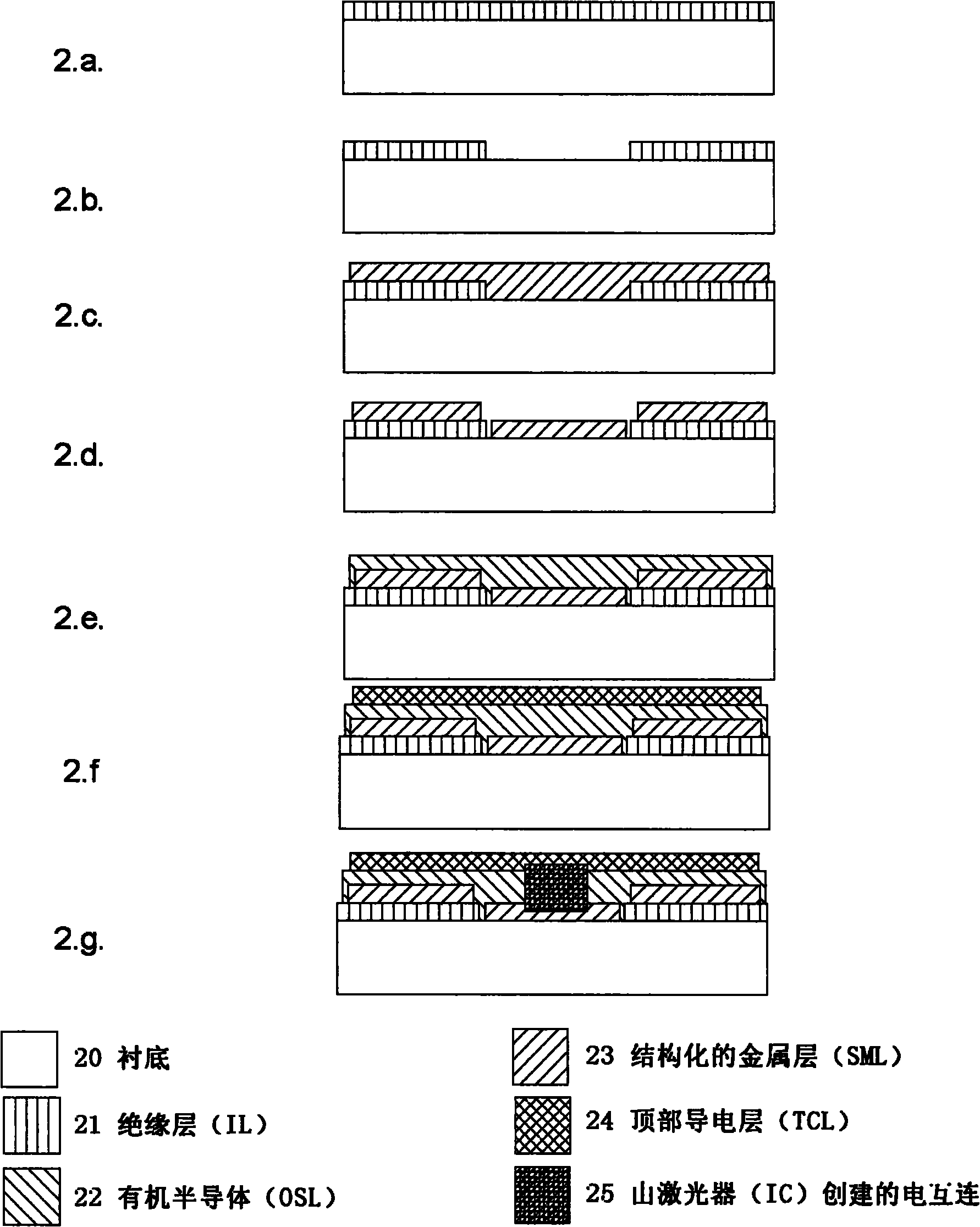
[0159] A 0.8 mm thick stainless steel plate having a lateral dimension of 100 mm×100 mm was provided as a substrate. A 2.3 μm thick polyimide layer (PI2555 from HD Microsystems) was deposited on the metal substrate by spin coating at 3500 rpm and heating at 180° C. for half an hour. Repeat the steps of Example 1) (the first one is expected: a glass substrate is provided). As expected, the device worked as in Example 1).
example 3
[0160] Example 3): Organic Light Emitting Devices and Electrical Interconnects on Metal Substrates
[0161] A 0.8 mm thick stainless steel plate having a lateral dimension of 100 mm×100 mm was provided as a substrate. The patterned non-conductive layer was deposited as explained above. like Figure 4 As shown, a 100 nm thick Ag SML layer was deposited on the polyimide layer (RA) and on the exposed substrate area (RB). In this case, the feed contact is provided by the substrate itself (region (RN)). As in Example 1), the steps of depositing OSL and TCL were repeated.
[0162] Electrical interconnections are formed by applying laser pulses on the region (RB); the laser is applied from the top side (in other words, not through the substrate). The laser used in this example was a pulsed Nd:YVO4 laser operating at 1064 nm. Interconnect points were fabricated over a length of 80 mm per region (RB) (this length overlapped with the OSL) with a line density of 1 dot / 250 μm.
[...
PUM
 Abstract
Description
Claims
Application Information
 - R&D
- Intellectual Property
- Life Sciences
- Materials
- Tech Scout
- Unparalleled Data Quality
- Higher Quality Content
- 60% Fewer Hallucinations
Browse by: Latest US Patents, China's latest patents, Technical Efficacy Thesaurus, Application Domain, Technology Topic, Popular Technical Reports.
© 2025 PatSnap. All rights reserved.Legal|Privacy policy|Modern Slavery Act Transparency Statement|Sitemap|About US| Contact US: help@patsnap.com