LVDS (Low Voltage Differential Signaling) driver

A driver and input buffer technology, applied in the field of electronics, can solve the problems of output change, impossible instantaneous conversion and timely response, etc., to reduce the gate voltage deviation and achieve the effect of dynamic stability

Active Publication Date: 2012-11-21
CHENGDU SINO MICROELECTRONICS TECH CO LTD
View PDF0 Cites 0 Cited by
  • Summary
  • Abstract
  • Description
  • Claims
  • Application Information

AI Technical Summary

Problems solved by technology

Since the Buffer has a certain settling response time, it is impossible to respond to the instantaneous conversion in time; in addition, the excess charge in the channel on the switch S1 / S2 will be injected into the Buffer output to make the output change

Method used


Image

  • LVDS (Low Voltage Differential Signaling) driver
  • LVDS (Low Voltage Differential Signaling) driver
  • LVDS (Low Voltage Differential Signaling) driver

Examples


Embodiment Construction

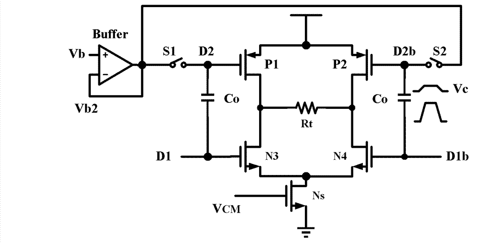
[0014] see figure 2 .

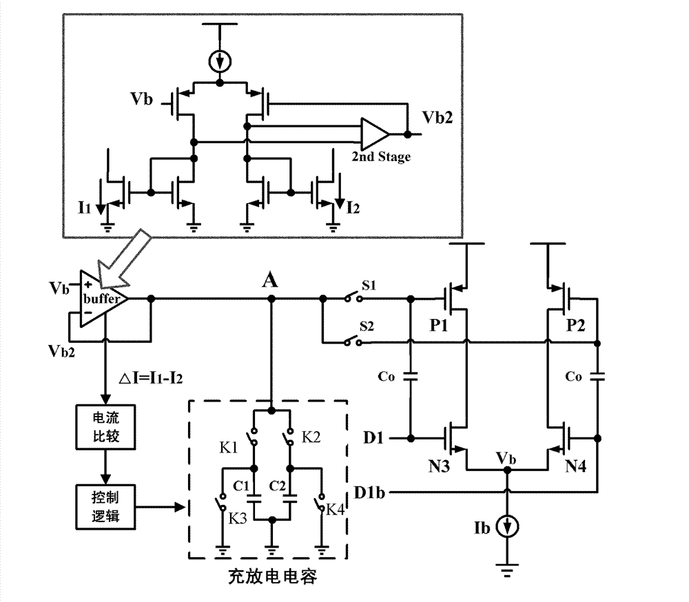
[0015] The LVDS driver of the present invention includes an input buffer unit and a drive unit, and also includes a charge and discharge control unit, and the charge and discharge control unit includes a voltage difference / current difference conversion unit, a current comparison unit, a control logic unit, and a charge and discharge unit; a current comparison unit The voltage difference / current difference conversion unit is connected to the input buffer unit; the control logic unit is connected to the current comparison unit, and is connected to the control terminal of the charging and discharging unit; the output terminal of the charging and discharging unit is connected to the output terminal of the input buffering unit. The charging and discharging unit includes a first capacitor branch and a second capacitor branch connected in parallel between the output terminal of the charging and discharging unit and the ground level, and the first capacitor br...


PUM


Abstract

The invention relates to an LVDS (Low Voltage Differential Signaling) driver, relating to electronic technologies. The LVDS driver comprises an input cache unit and a drive unit. The LVDS driver is characterized by also comprising a charge and discharge control unit, wherein the charge and discharge control unit comprises a voltage difference / current difference converting unit, a current comparing unit, a control logic unit and a charging and discharging unit; the current comparing unit is connected with the input cache unit through the voltage difference / current difference converting unit; the control logic unit is connected with the current comparing unit and is also connected with the control end of the charging and discharging unit; and the output end of the charging and discharging unit is connected with the output end of the input cache unit. The invention has the advantages of reducing the grid voltage deviation of a driving circuit and realizing dynamic stabilization.

Description

technical field [0001] The present invention relates to electronic technology, in particular to integrated circuit technology. Background technique [0002] Existing technologies such as figure 1 As shown, when D1 is "low" and D1b is "high", N3 is turned off and N4 is turned on; switch S2 is turned off, and S1 is closed so that the Buffer output Vb2 is connected to the gate of P1, so that P1 is in a normal working state. Its gate voltage Vb2=Vb. And because of the effect of Co, the gate voltage on P2 is VC so that P2 is turned off. In this way, the 3.5mA current will flow through the terminal resistor Rt to generate a standard LVDS signal, and the output common mode voltage is adjusted by the common mode feedback circuit to stabilize the gate voltage VCM of Ns, which is about 1.2V. When D1 is "high" and D1b is "low", contrary to the above situation, the N3 and P2 transistors are turned on to reverse the current flowing through Rt. [0003] However, in the case of high fr...

Claims


Application Information

Patent Timeline
Patent Type & Authority Patents(China)
IPC IPC(8): H03K19/0175
Inventor 蔡化岑远军朱志勇张克林
Owner CHENGDU SINO MICROELECTRONICS TECH CO LTD
Why Eureka
Try Eureka