Semiconductor circuit assembly

A circuit layout and semiconductor technology, applied in the direction of semiconductor devices, circuits, conductive connections, etc., can solve the problems of not always ensuring the contact of the contact section, interference with electrical contact, heating, etc., and achieve the goal of not easy to interfere, simple cost, and high current-carrying capacity Effect

Inactive Publication Date: 2011-08-17
SEMIKRON ELECTRONICS GMBH & CO KG
View PDF1 Cites 4 Cited by
  • Summary
  • Abstract
  • Description
  • Claims
  • Application Information

AI Technical Summary

Problems solved by technology

[0004] In the known electrical contact connection between the first contact section and the second contact section, depending on the construction, it is not always possible to ensure full-surface contact between the contact sections.
This leads to undesired heatin

Method used


Image

  • Semiconductor circuit assembly
  • Semiconductor circuit assembly
  • Semiconductor circuit assembly

Examples


Embodiment Construction

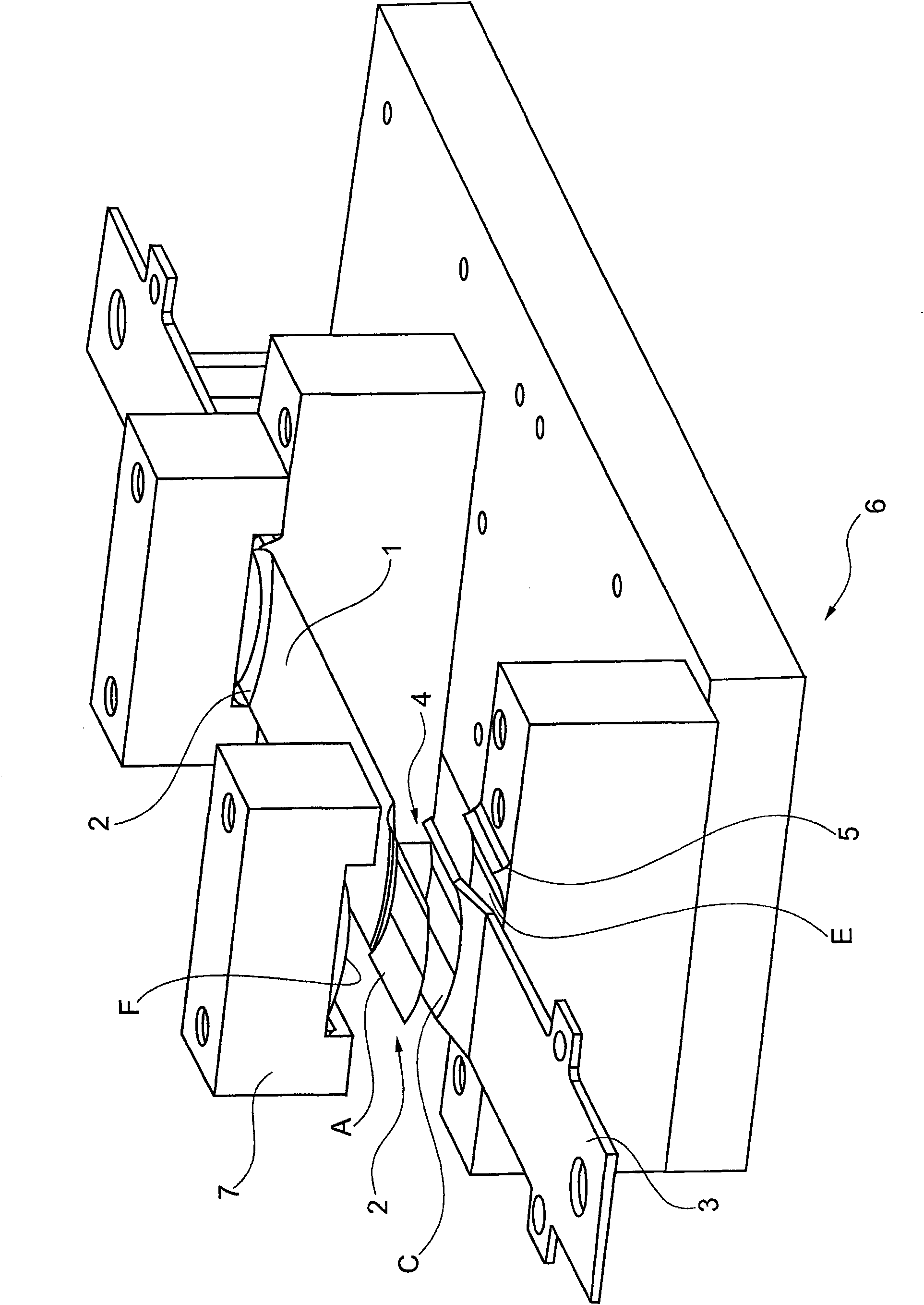
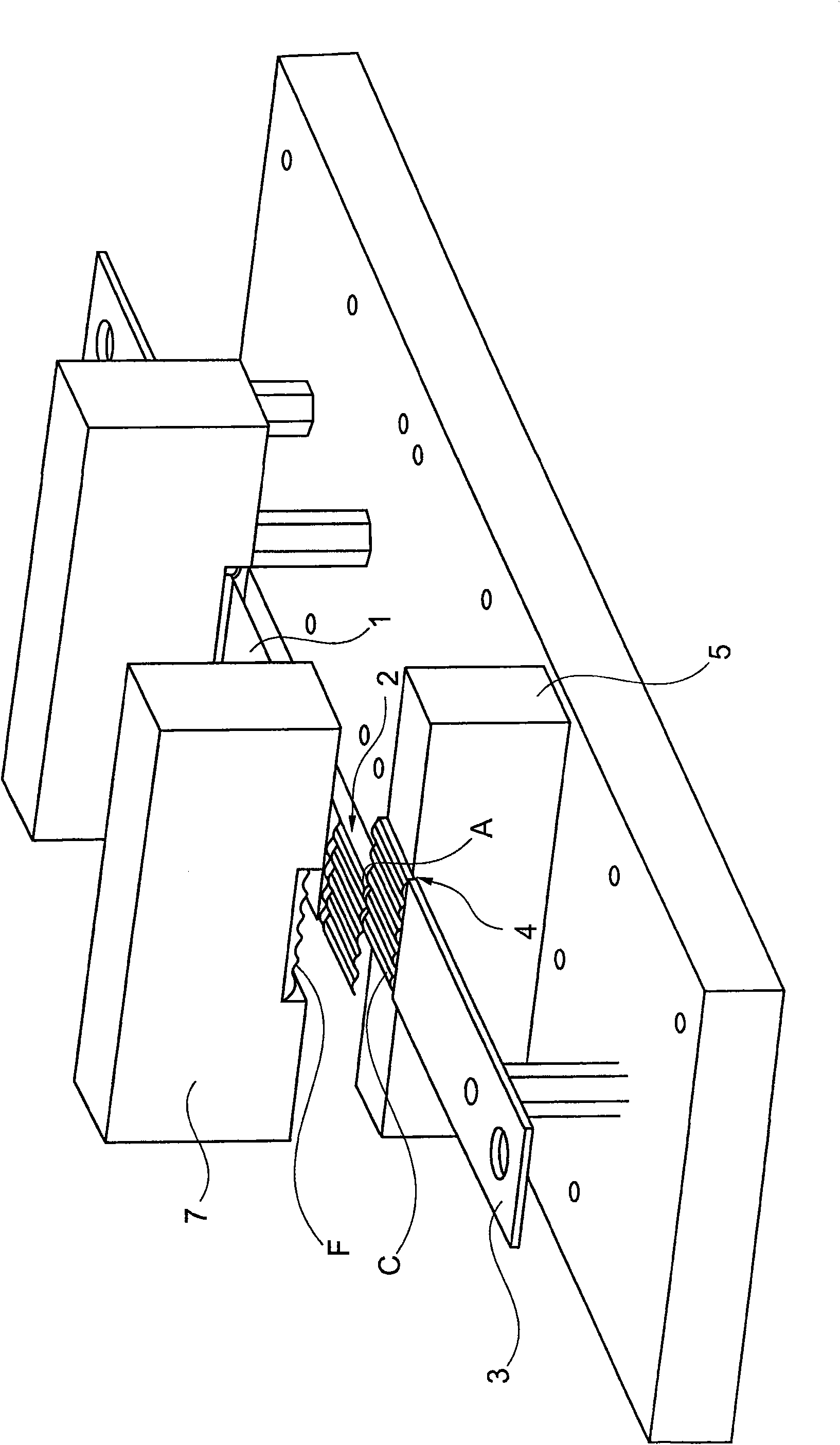
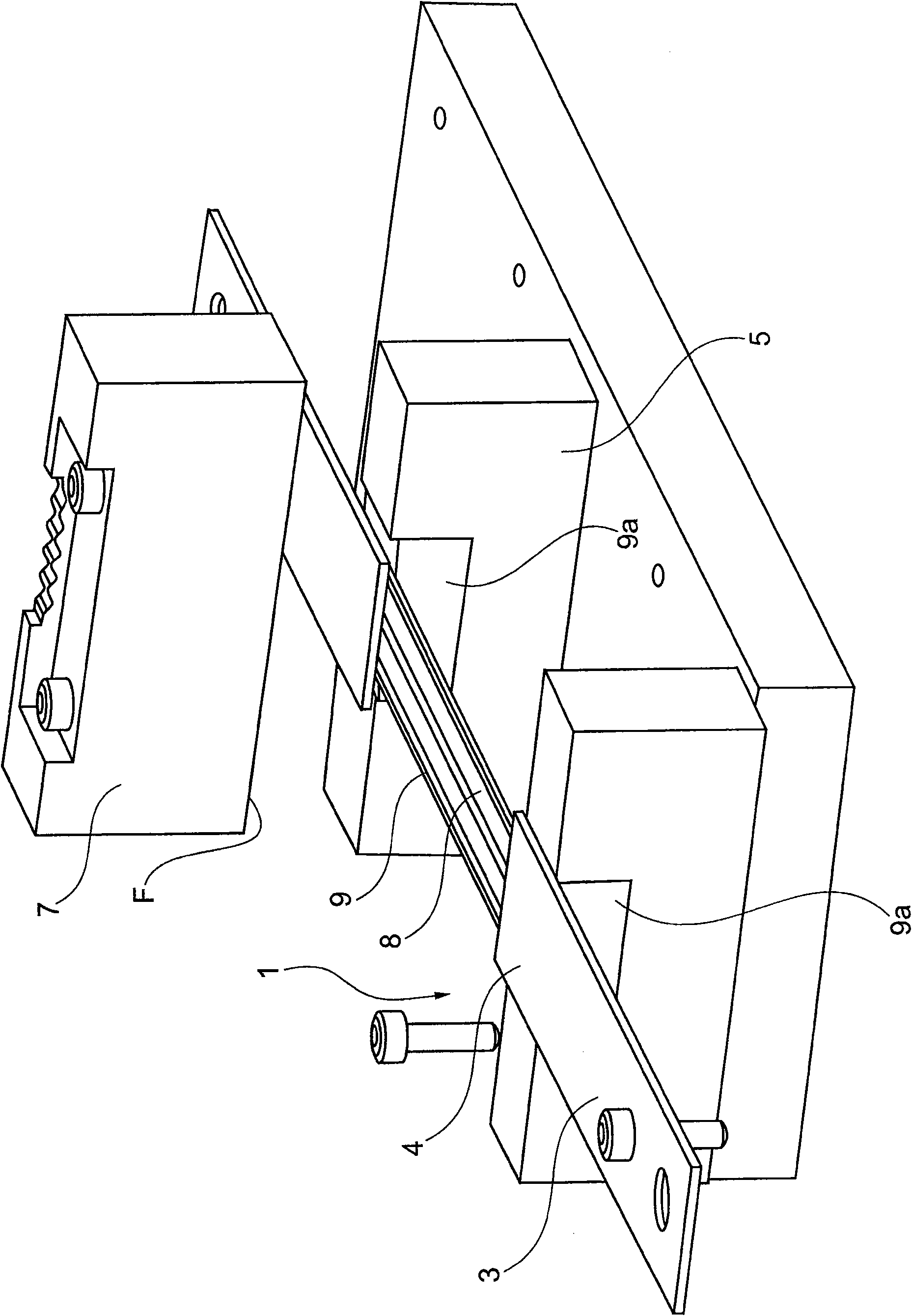
[0023] exist figure 1 In , the reference numeral 1 is used to designate the connecting device, which is formed from a film composite structure. The film composite comprises at least one electrically insulating film made of plastic, which has metallization on at least one side. The metallization can be configured, for example, in the form of conductor tracks. Of course, this metallization can be provided on both sides of the electrically insulating plastic film. The reference number 2 is used to designate the first contact section of the thin-film composite structure 1 . In the region of the first contact section, the metallization is exposed, but it can otherwise be covered by another layer of insulating plastic for insulation purposes. as from figure 1 As can be seen, the connecting device can also have two first contact sections 2 at its two ends. The first contact section 2 has a first contact surface A and an opposite (not visible here) second contact surface B. FIG. ...


PUM


Abstract

The invention relates to a semiconductor circuit assembly which comprises a connecting device (1) provided with a first contact section (2) and formed from a composite film, a connection element (3) provided with a second contact section (4), a housing including a counter bearing (5) for supporting one of the contact sections (2, 4), and a mechanism generating clamping force to forcing the contact section (4) abut against each other. In order to improve the flow bearing capacity of the contact, the first contact section (2) and or the second contact section (4) and/or the counter bearing (5) include respective contact areas (A, B, C, D, E, F), where the contact areas are different from each other. One of the superimposed arranged contact sections (2, 4) deforms when exercising clamping force, where the section is adapted to shape of the other contact section during an electrical contact.

Description

technical field [0001] The invention relates to a semiconductor circuit arrangement according to the preamble of claim 1 . Background technique [0002] Such a semiconductor circuit arrangement is known, for example, from DE 10 2006 027 482 B3. In known semiconductor circuit arrangements, connecting devices are used for connecting contact elements arranged on the substrate to connection elements for connecting external load connections. This is a flexible film composite structure in which conductor tracks are applied to the top and bottom of an electrically insulating film made of plastic. The conductor tracks are connected to the contacts provided on the substrate, for example by means of soldering. [0003] In order to make electrical contact with the terminal element, the terminally arranged first contact section of the connection device is supported on a support arranged in the region of the housing wall. A curved spring element accommodated in a housing recess urges ...

Claims


Application Information

Patent Timeline
IPC IPC(8): H01L23/498H01L23/10
CPCH01R4/182H01R4/188H01R12/592
Inventor 英戈・博根
Owner SEMIKRON ELECTRONICS GMBH & CO KG
Why Eureka
Try Eureka