Apparatus for processing and observing a sample

a technology for processing and observing samples, applied in the field of sample manufacturing apparatuses, can solve problems such as difficult interference between the sample holder for observation and the sample stage, and achieve the effects of compact device, preventing interference, and compact devi

Inactive Publication Date: 2005-03-22
HITACHI HIGH TECH SCI CORP
View PDF1 Cites 24 Cited by
  • Summary
  • Abstract
  • Description
  • Claims
  • Application Information

AI Technical Summary

Benefits of technology

In order to achieve the above described object, a sample manufacturing device of the present invention comprises a sample stage to which an original sample is fixed, a focused ion beam irradiation system for irradiating a focused ion beam from a vertical direction to a specified place on the original sample fixed to the sample stage, and a side entry stage, arranged diagonally above the sample stage, for inserting a sample holder for specified observation in a diagonal direction with respect to the vertical direction, and supporting the inserted sample stage for observation so as to be capable of movement in the diagonal direction, wherein a test piece taken out from a specified place of the original sample is fixed to a tip section of the sample holder for specified observation supported on the side entry stage. With this structure, the sample holder for observation is configured so as to be inserted diagonally from above the sample stage, which means that compared to the related art where the sample holder is inserted in a horizontal direction, it is difficult for interference to arise between the sample holder for observation and the sample stage.
In the case described above, the side entry stage preferably has the sample holder for specified observation held so that a tip of the sample holder for specified observation is positioned in a space formed by removing the original sample from on the sample stage, and is further provided with a manipulator attached to a tip of the sample holder for specified observation held on the side entry stage for removing the test piece from a specified place on the original sample. With this structure, using a space made by removing the sample holder for specified observation to which the original sample is fixed from on the sample stage, the test piece is fixed to the sample holder for specified observation, which means that the sample stage can be made to retreat from the FIB processing position in order to prevent interference. In this way, according to this structure, the movement space for the sample stage (retreat space) that was required in the related art is no longer required, which means the device can be made more compact to the extent of that space.
Further, the sample holder for specified observation is provided with a needle on a tip, and the side entry stage is preferably configured so that the sample holder for specified observation is moved three dimensionally to cause the tip of the needle to come into contact with or approach a specified location of the original sample. In this configuration also, since the movement space for the sample stage for preventing interference that is required in the related art is no longer required, it is possible to make the device more compact to the extent of that space. In addition, since the manipulator is not required, it is possible to make the device compact and also to reduce cost by that extent.
In the invention described above, the focused ion beam irradiation system preferably has a structure comprising a lens barrel provided with first and second irradiation systems, the lens barrel being attached to a sample chamber housing the sample stage, and is further provided with a lens barrel internal entry stage, attached to the lens barrel at an outer side of the sample chamber, into which the sample holder for specified observation is inserted, the first irradiation system irradiating an ion beam to a specified place on the original sample fixed to the sample stage, and the second irradiation system irradiating an ion beam to the test piece fixed to a tip of the sample holder for specified observation inserted from the lens barrel internal entry stage. In this case, by using the lens barrel internal entry stage, processing precision of the test piece is improved.

Problems solved by technology

With this structure, the sample holder for observation is configured so as to be inserted diagonally from above the sample stage, which means that compared to the related art where the sample holder is inserted in a horizontal direction, it is difficult for interference to arise between the sample holder for observation and the sample stage.

Method used


Image

  • Apparatus for processing and observing a sample
  • Apparatus for processing and observing a sample
  • Apparatus for processing and observing a sample

Examples


embodiment 1

(Embodiment 1)

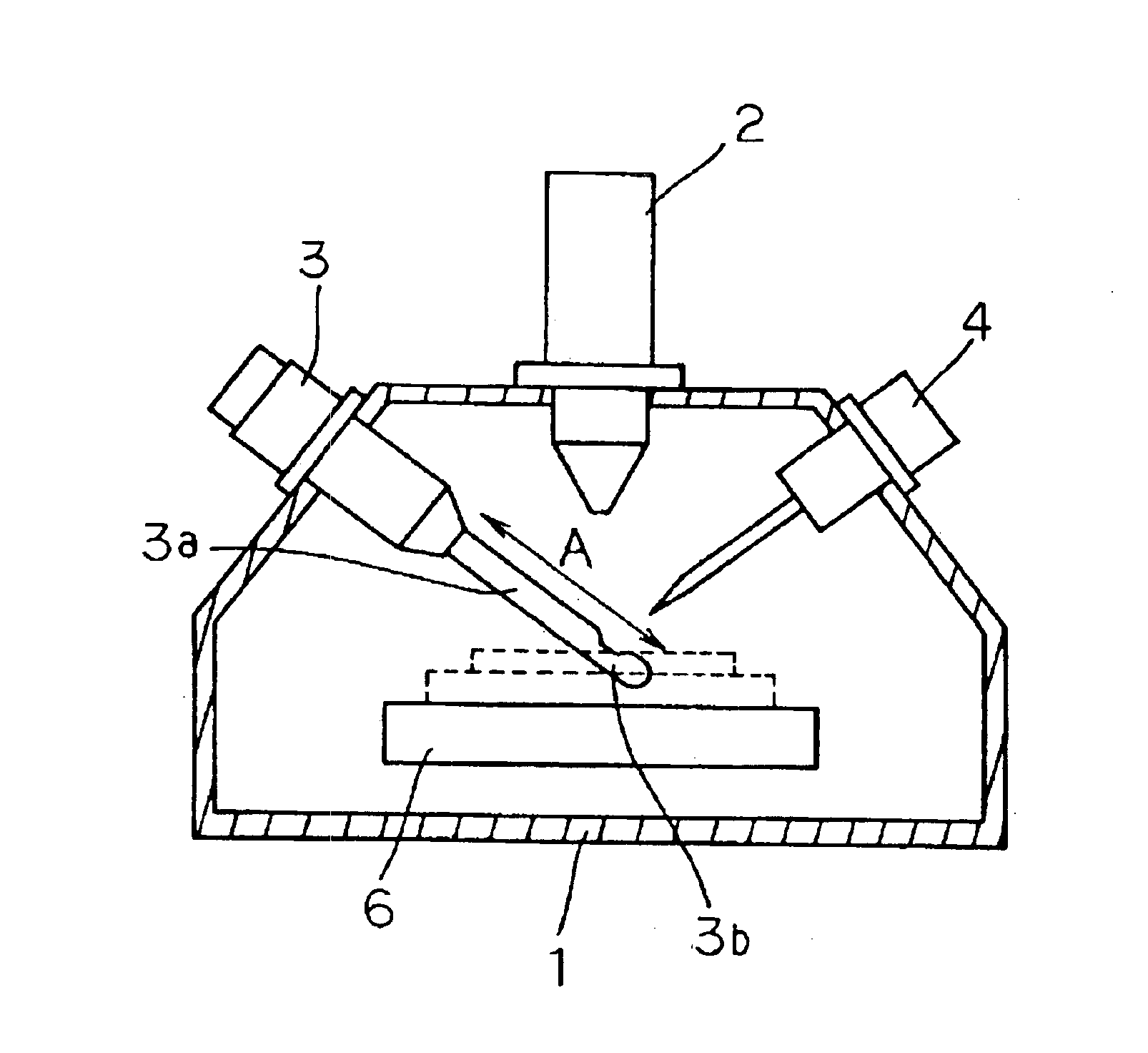
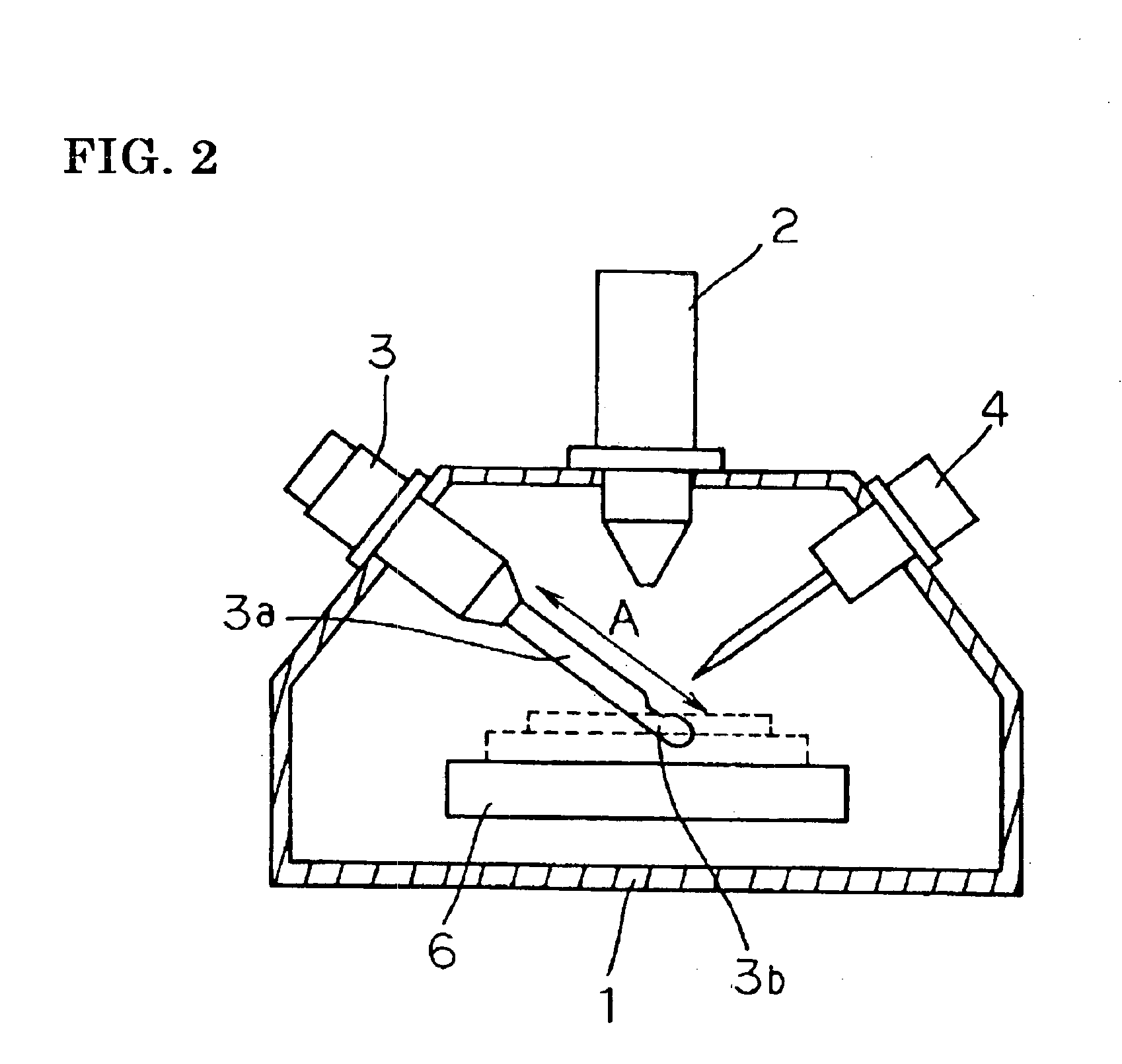
FIG. 1 is a schematic cross sectional view showing the schematic structure of an FIB device of a first embodiment of a sample manufacturing device of the present invention. This FIB device is for manufacturing a test piece such as a TEM sample or an SEM sample from a wafer, being an original sample, using a pick-up method, and is provided with a sample chamber 1 that is evacuated using an evacuation pump, not shown, with an FIB irradiation optical system 2, a side entry stage 3, a manipulator 4 and a sample stage 6 being provided in this sample chamber 1. Besides this, although not shown in FIG. 1, structures required for FIB processing, such as a gas gun and a secondary charged particle detector, are also provided in the sample chamber 1.

A sample holder 5 for fixing an original sample 7, being a wafer, and the sample stage 6 are the same as shown in FIG. 10. The FIB irradiation optical system 2 is positioned above the sample stage 6, and can scan a specified location ...

embodiment 2

(Embodiment 2)

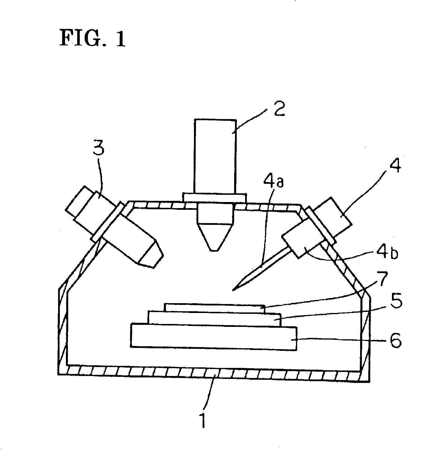
With the above described first embodiment, a test piece (TEM sample or SEM sample) was taken out from the wafer, (being the original sample) using a manipulator, but it is also possible to take out the test piece with the observation sample holder itself, without using the manipulator. Here, description will be given for the state where it is possible to take out the test piece using the observation sample holder itself.

FIG. 7 is a schematic cross sectional drawing of the outline structure of an FIB device of a second embodiment of a sample manufacturing device of the present invention. With this FIB device, the manipulator is done away with from the structure shown in FIG. 1, and a TEM sample holder 40 having a needle 41 detachably provided on a tip section is attached to the side entry stage 3. In FIG. 7, the same reference numerals are attached to parts that are the same as in FIG. 1.

The needle 41 has a tapered tip, and an end opposite to the tip is fixed to the TEM...

embodiment 3

(Embodiment 3)

FIG. 9 is a schematic cross sectional drawing of the outline structure of an FIB device of a third embodiment of a sample manufacturing device of the present invention. With this FIB device, the FIB irradiation optical system 2 is done away with from the structure shown in FIG. 1, and apart from provision of an FIB irradiation optical system 20 having a lens barrel internal side entry stage 21, it is the same as the FIB device of the first embodiment described above.

The FIB irradiation optical system 20 is similar to the FIB irradiation optical system 2 shown in FIG. 1, and is attached to the sample chamber 1 so that it is possible to irradiate a specified location of an original sample 7 mounted on the sample stage 6 via the sample holder 5 with an ion beam, with the lens barrel internal side entry stage 21 being attached to a specified place of the lens barrel. The lens barrel internal side entry stage 21 can have an observation sample holder 22, constituted by the T...


PUM

PropertyMeasurementUnit
thicknessaaaaaaaaaa
microscopeaaaaaaaaaa
transmission electron microscopeaaaaaaaaaa

Abstract

An apparatus for processing and observing a sample has a sample stage for supporting a sample at a preselected location thereof, a focused ion beam irradiation system for irradiating the sample with a focused ion beam along an optical axis to cut out a portion from the sample, and a side entry stage disposed over the sample stage and extending slantingly with respect to the optical axis of the focused ion beam irradiated by the focused ion beam irradiation system. The side entry stage has a microscope sample holder for picking up the cut-out sample portion directly from the preselected location of the sample and for supporting the sample portion. The microscope sample holder is configured to be removed from the side entry stage while supporting the sample portion and to be connected to an entry stage of a microscope device for observing the sample portion.

Description

BACKGROUND OF THE INVENTION1. Technical FieldThe present invention relates to a sample manufacturing apparatus and, more specifically, to an apparatus for making test pieces for slice observation from a wafer with a transmission electron microscope (hereafter referred to as TEM) or a scanning electron microscope (hereafter referred to as SEM) utilizing ultra-fine processing using a focused ion beam (hereafter referred to as FIB).2. Related ArtAn FIB device is known as a device for manufacturing a test piece such a TEM sample or an SEM sample from a wafer, being an original sample. A schematic drawing of an FIB device of the related art is shown in FIG. 10. The main components of this FIB device are an ion source 100, an ion optical system 101, a secondary charged particle detector 102, a gas gun 103, a sample holder 104 and a sample stage 105.The ion source 100 is a liquid metal ion source exemplified by, for example, gallium (Ga). The ion optical system 101 is for focusing an ion b...

Claims


Application Information

Patent Timeline
Patent Type & Authority Patents(United States)
IPC IPC(8): G01N1/28H01J37/20H01J37/305
CPCG01N1/286H01J37/3056H01J37/20G01N2001/2873H01J2237/31745H01J2237/2817
Inventor ADACHI, TATSUYAFUJII, TOSHIAKISAWARAGI, HIROSHISUGIYAMA, YASUHIKO
Owner HITACHI HIGH TECH SCI CORP
Why Eureka
Try Eureka