Epitaxial growth method of W type antimonide class II quantum well

An epitaxial growth and quantum well technology, applied in the semiconductor field, can solve the problems of immature semiconductor optoelectronic devices and wide band gap.

Active Publication Date: 2011-08-17
INST OF SEMICONDUCTORS - CHINESE ACAD OF SCI
View PDF4 Cites 12 Cited by
  • Summary
  • Abstract
  • Description
  • Claims
  • Application Information

AI Technical Summary

Problems solved by technology

Traditional Si-based and GaAs-based materials have relatively wide band gaps, which cannot meet the requirements for wavelengths, while antimonide (GaSb-based) materials have relatively narrow band gaps, so they have become the main research objects in this band.
At present, no matter in terms of materials or devices, semiconductor optoelectronic devices in the mid-infrared 2-5μm band are not mature enough.

Method used


Image

  • Epitaxial growth method of W type antimonide class II quantum well
  • Epitaxial growth method of W type antimonide class II quantum well
  • Epitaxial growth method of W type antimonide class II quantum well

Examples


Embodiment Construction

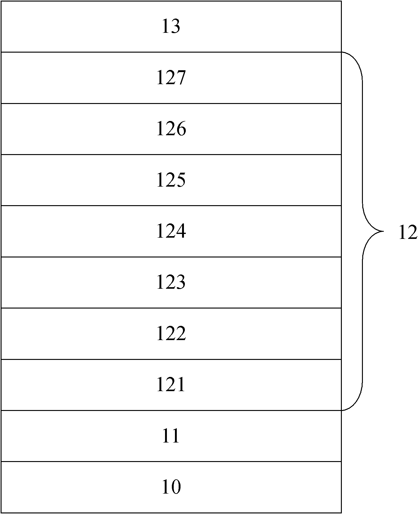
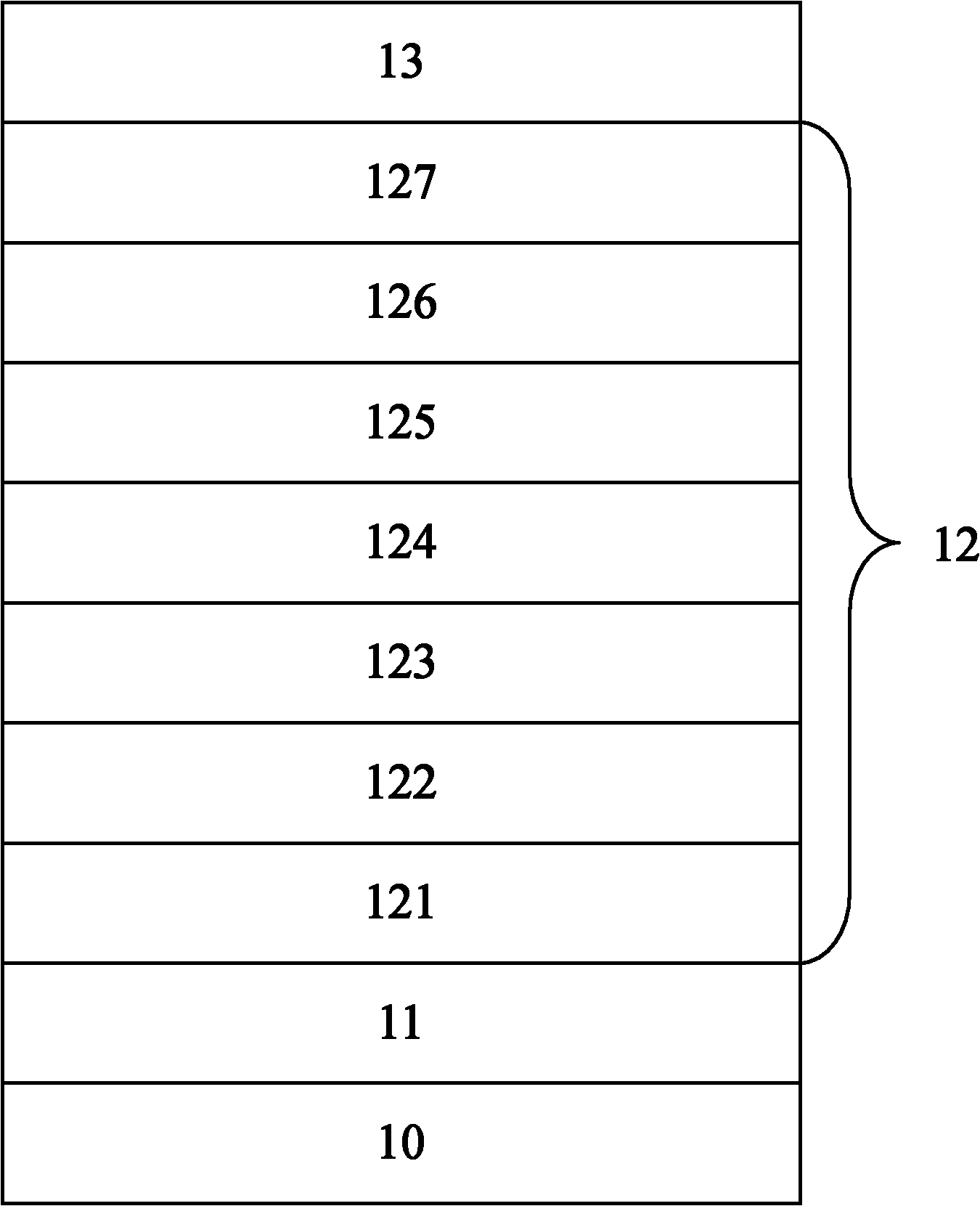
[0019] see figure 1 As shown, the present invention provides an epitaxial growth method of a "W" type antimonide type II quantum well, comprising the following steps:

[0020] Step 1: select a substrate 10, the substrate 10 is a GaSb (001) substrate;

[0021] Step 2: Deoxidize and degas the substrate 10 and observe the surface reconstruction, which means that the temperature of deoxidation is 630°C, then the temperature is raised to 660°C for degassing, and after 15 minutes, the temperature is lowered to 610°C, and GaSb is grown for 5 minutes. After cooling to 490°C, reconstitution was observed.

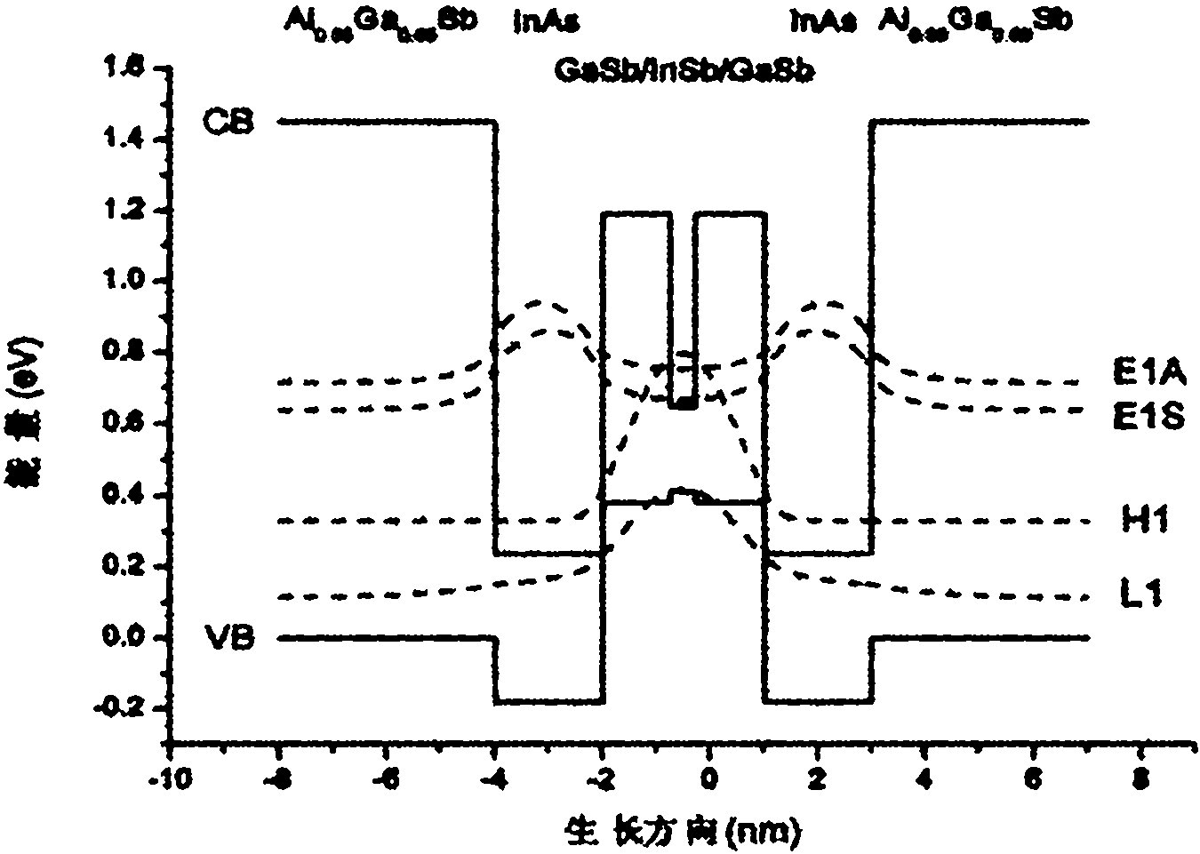
[0022] Step 3: A buffer layer 11, a 10-cycle “W” structure type II quantum well active region 12 and a GaSb cap layer 13 are sequentially grown on the substrate 10. The buffer layer 11 is made of GaSb, and the 10 Each period of the "W" structure type II quantum well active region 12 includes: an Al 0.35 Ga 0.65 Sb barrier layer 121, growth time 16s, thickness 4nm, this layer and ...


PUM


Abstract

The invention relates to an epitaxial growth method of a W type antimonide class II quantum well, which comprises the following steps: step 1) selecting a substrate; step 2) performing deoxidation and degasification treatment on the substrate, and observing the surface reconstruction; and step 3) sequentially growing a buffer layer, a W-structured class II quantum well active area with 10 cycles and a GaSb cover layer on the substrate.

Description

technical field [0001] The invention relates to the technical field of semiconductors, and mainly relates to a method for growing a two-type "W" type quantum well structure on a GaSb substrate. Background technique [0002] With the development of science and technology, semiconductor lasers in the mid-infrared 2-5μm band have received more and more attention. The main applications are chemical gas detection, communication, biomedicine and military electronic countermeasures. The traditional Si-based and GaAs-based materials have relatively wide band gaps and cannot meet the requirements for wavelength, while antimonide (GaSb-based) materials have relatively narrow band gaps, thus becoming the main research object in this band. At present, both in terms of materials and devices, semiconductor optoelectronic devices in the mid-infrared 2-5μm band are not mature enough. [0003] At present, there are many research directions in the mid-infrared band. In the 2-3 μm band, a cl...

Claims


Application Information

Patent Timeline
Patent Type & Authority Applications(China)
IPC IPC(8): H01S5/343C30B25/20
Inventor 迂修张宇王国伟徐应强徐云宋国峰
Owner INST OF SEMICONDUCTORS - CHINESE ACAD OF SCI
Why Eureka
Try Eureka