Impulse modulation method and circuit for switch transistor drive signals
A technology for switching transistors and driving signals, applied in the field of pulse modulation circuits, can solve problems such as increasing development difficulty and rising cost, and achieve the effects of reduced development cost and development difficulty, fewer components, and low cost
- Summary
- Abstract
- Description
- Claims
- Application Information
AI Technical Summary
Problems solved by technology
Method used
Image

Examples
Embodiment 1
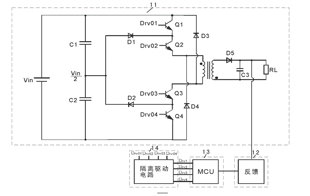
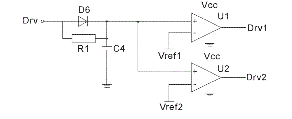
[0040] Embodiments of the present invention are as Figure 4 As shown, the three-level two-transistor flyback main power circuit, the feedback circuit, the control IC, the pulse modulation circuit, and the isolation drive circuit are sequentially connected to form a two-transistor three-level flyback converter, wherein the pulse modulation circuit (such as figure 2shown) includes a switching diode D6, an RC charging and discharging circuit composed of a resistor R1 and a capacitor C4, a voltage comparator U1 and a voltage comparator U2;
[0041] The anode of the switching diode D6 is connected to the PWM output pin Drv of the PWM control IC to input pulses, the cathode of the switching diode D6 is connected to the non-inverting input terminals of the voltage comparator U1 and the voltage comparator U2, and the resistor R1 is connected in parallel to the positive of the diode D6 Between the negative poles, one end of the capacitor C4 is connected to the negative pole of the di...
Embodiment 2
[0059] Such as Figure 5 Shown is the circuit schematic diagram of Embodiment 2 of the present invention. The difference from Embodiment 1 is that a pull-up resistor R2, R3, to improve the drive capability of the circuit.
Embodiment 3
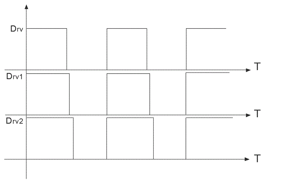
[0061] Such as Figure 6 As shown, in order to further improve the present invention, on the basis of Embodiment 1, the pulse modulation circuit of the present invention adds n (n=1, 2...) voltage comparators, wherein, the non-inverting input terminal of the voltage comparator Un is connected in parallel On the non-inverting input terminal of the voltage comparator U1 or the voltage comparator U2, the inverting input terminal of the voltage comparator Un is connected to the corresponding reference voltage Vrefn, and the modulated output pulse Drvn is output through the pulse output terminal, and each voltage comparator The output terminals can realize the output pulse drive signal with rising edge synchronization and falling edge delay sequentially, and each output pulse is output to the isolation drive circuit.
PUM
 Abstract
Description
Claims
Application Information
 - R&D
- Intellectual Property
- Life Sciences
- Materials
- Tech Scout
- Unparalleled Data Quality
- Higher Quality Content
- 60% Fewer Hallucinations
Browse by: Latest US Patents, China's latest patents, Technical Efficacy Thesaurus, Application Domain, Technology Topic, Popular Technical Reports.
© 2025 PatSnap. All rights reserved.Legal|Privacy policy|Modern Slavery Act Transparency Statement|Sitemap|About US| Contact US: help@patsnap.com