Touch panel and its display device, method of driving touch panel, and electronic device
A technology for a display device and a display part, applied in the fields of touch panels and display devices, drivers, and electronic devices, capable of solving problems such as increasing the aperture ratio of the display device and reducing the aperture ratio of the display device, and achieving the effect of high sensitivity
- Summary
- Abstract
- Description
- Claims
- Application Information
AI Technical Summary
Problems solved by technology
Method used
Image
Examples
no. 1 approach
[0062] (Structure example)
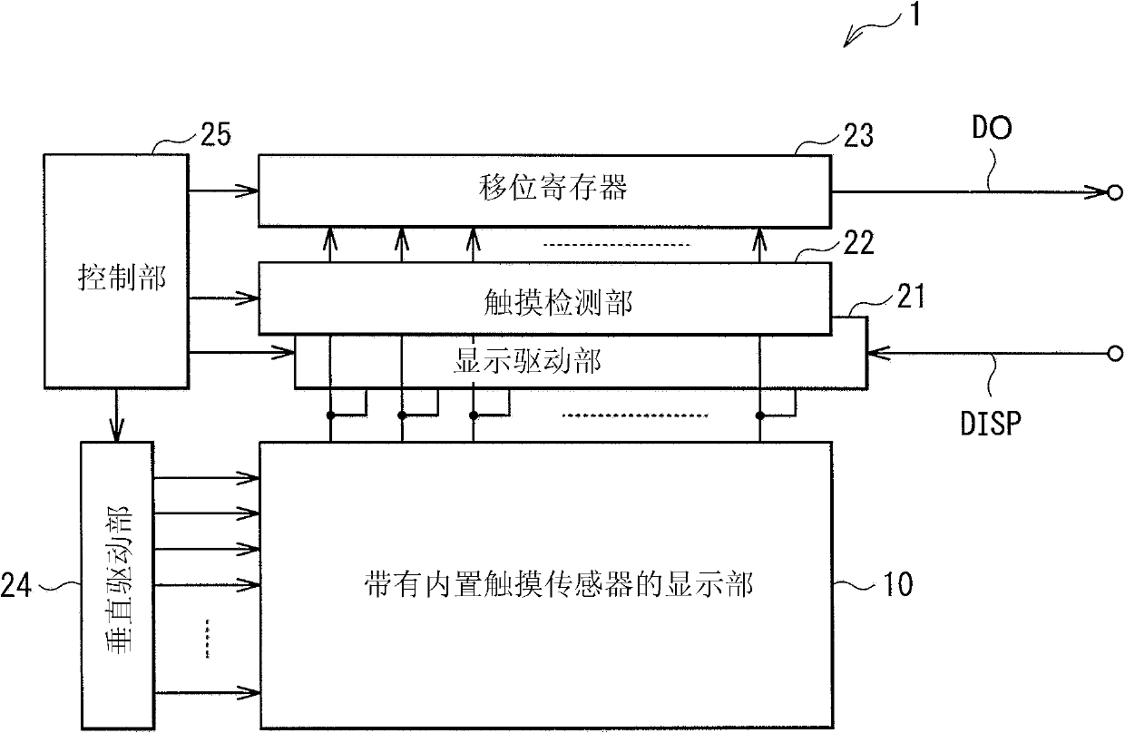
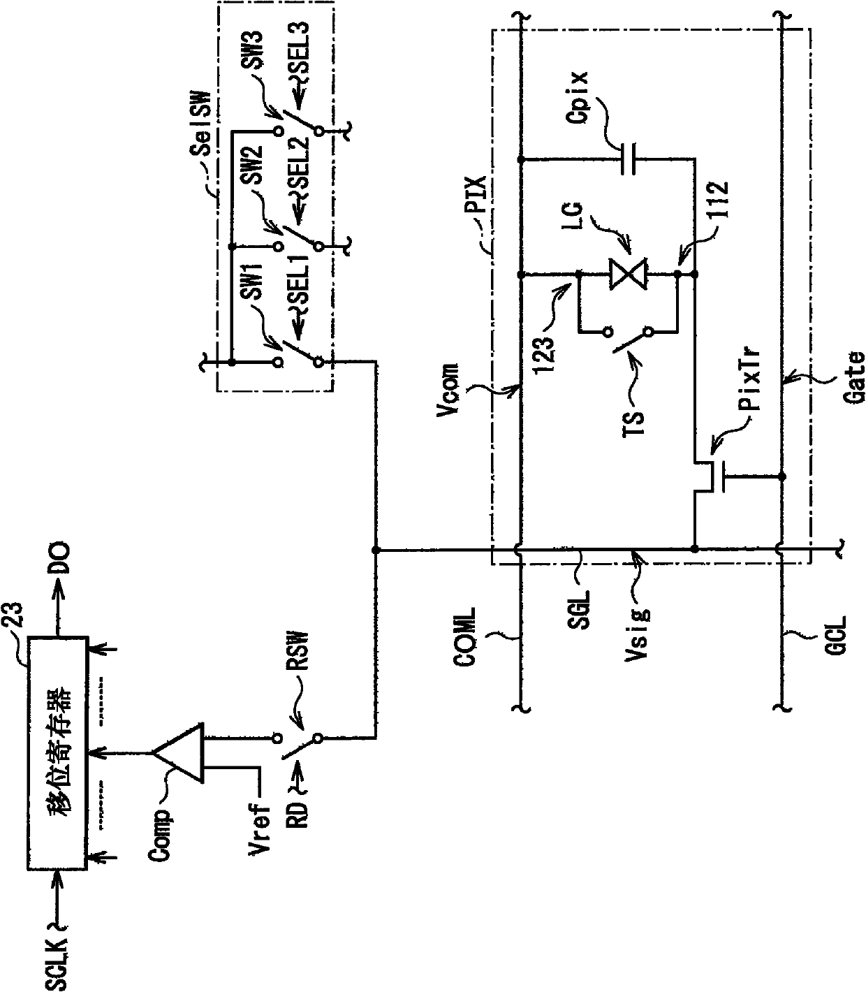
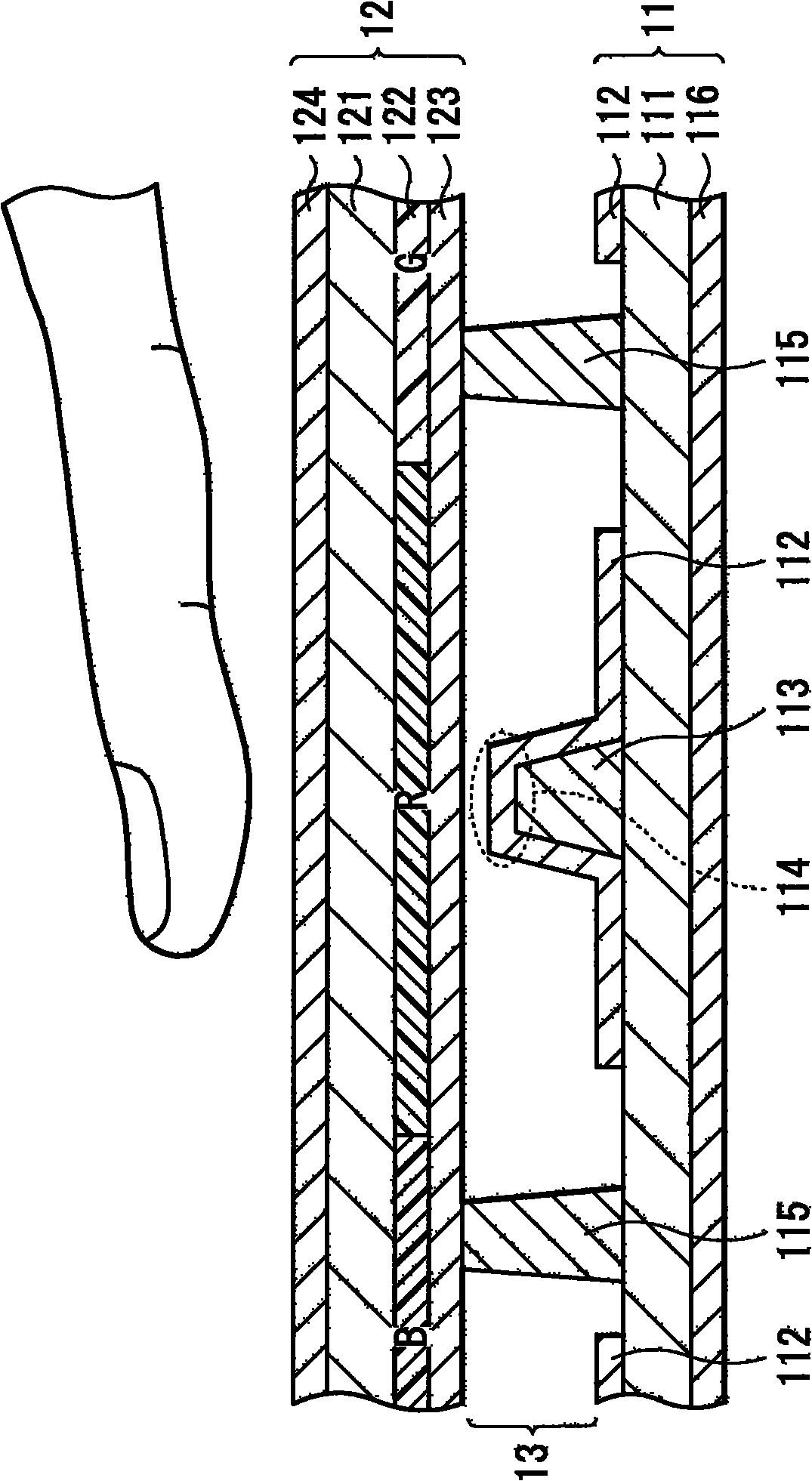
[0063] figure 1 A structural example of a display device with a touch sensor according to the first embodiment of the present disclosure is shown. figure 2 A structural example of a main part of a display device with a touch sensor is shown. Since the method of driving the touch panel according to the embodiment of the present disclosure is implemented through this embodiment, a description thereof will be additionally given in this embodiment. The display device 1 with a touch sensor is a so-called in-cell display device integrating a display panel and a touch panel. The display device 1 with a touch sensor uses a liquid crystal element as a display element, and is configured by using a contact type touch sensor and a capacitive type touch sensor as touch sensor elements. Such as figure 1 As shown, the display device 1 with a touch sensor includes a display unit with a built-in touch sensor 10 , a display drive unit 21 , a touch detection uni...
Deformed example 1-1
[0149] In the above-mentioned embodiments, although the display unit 10 with a built-in touch sensor is figure 2 The minimum components necessary and the minimum wiring necessary are shown, but the disclosure is not limited thereto. In this way substitution, for example, as in Figure 7 As shown, the display unit 10 with a built-in touch sensor can be configured by adding a sensor control line SCL.
[0150] Although one end of the pixel capacitor Cpix is connected to figure 2 In the common signal line COML, but in the alternative of this way, one end of the pixel capacitance Cpix can be connected to Figure 7 The sensor control line SCL in. The sensor control line signal Vse is supplied to the sensor control line SCL. The sensor control line signal Vse has the same waveform as the common signal Vcom, and the voltage magnitude of the sensor control line signal Vse is greater than that of the common signal Vcom.
[0151] Figure 8 A timing waveform diagram of a display...
no. 2 approach
[0154] Next, a display device with a touch sensor according to a second embodiment of the present disclosure will be described. In this embodiment, the method of driving the gate line GCL by the vertical driving section 24 is different from that of the first embodiment. In other words, in the first embodiment, although the vertical drive section 24 triggers the gate line signal Gate to one gate line GCL in periods other than the pixel electrode precharge period in each horizontal line period (1H), In the display device 1B with a touch sensor of this embodiment, the vertical driving section 24 triggers the gate line signal Gate to two or more gate lines GCL. The circuit structure of the display device 1B with a touch sensor of this embodiment is the same as that of the first embodiment ( figure 1 and figure 2 ), and the vertical driving section 24 drives the gate line GCL as described above. Other operations are the same as the first embodiment ( Figure 5 ) in the same wa...
PUM
 Abstract
Description
Claims
Application Information


