Pixel structure
A pixel structure and pixel electrode technology, applied in optics, instruments, electrical components, etc., can solve problems such as water ripples on the display screen, changes in the capacitance value of SMII storage capacitors, and afterimages.
- Summary
- Abstract
- Description
- Claims
- Application Information
AI Technical Summary
Problems solved by technology
Method used
Image

Examples
Embodiment Construction
[0047] The present invention will be described in detail below in conjunction with the accompanying drawings and specific embodiments, but not as a limitation of the present invention.
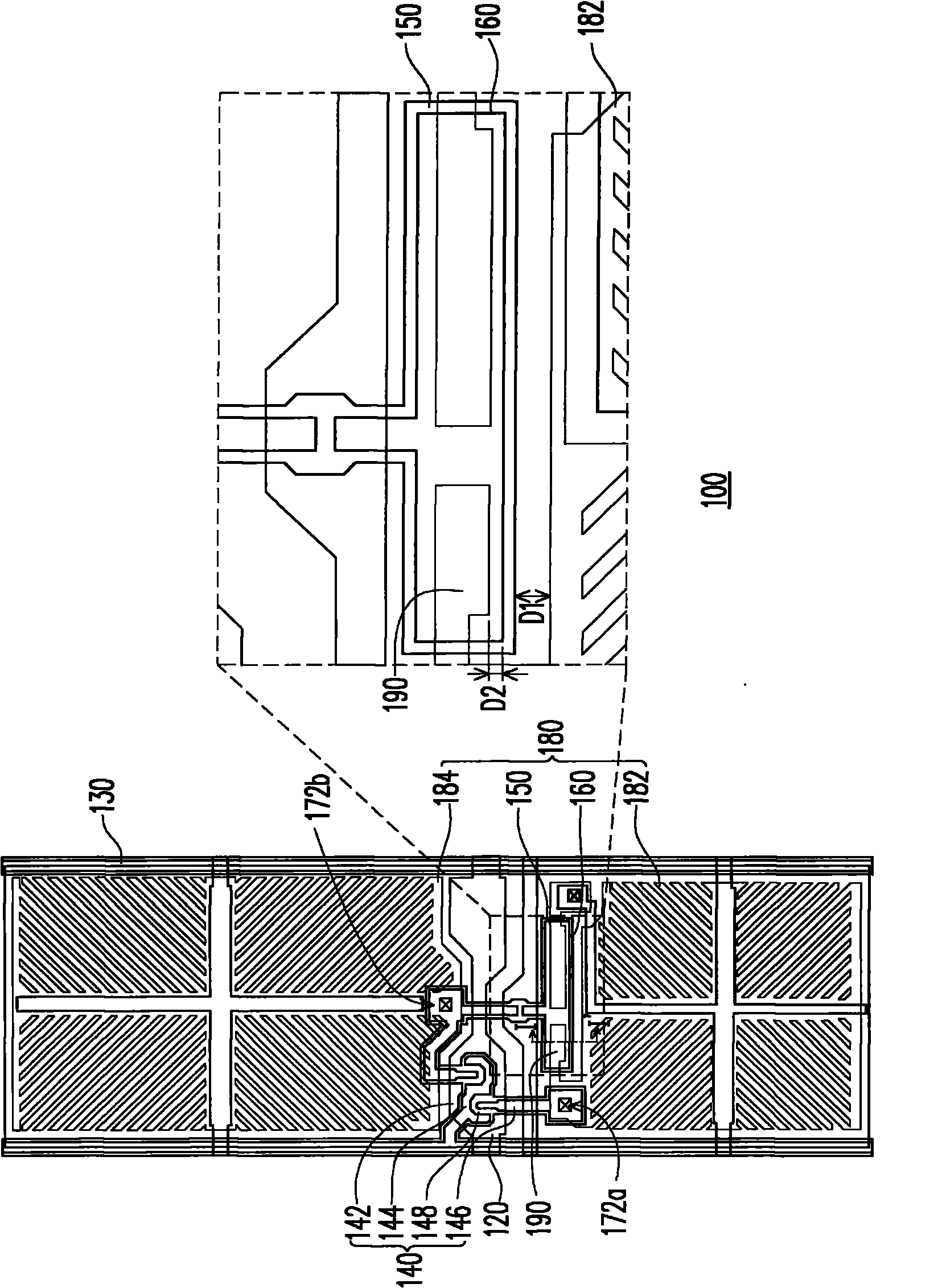
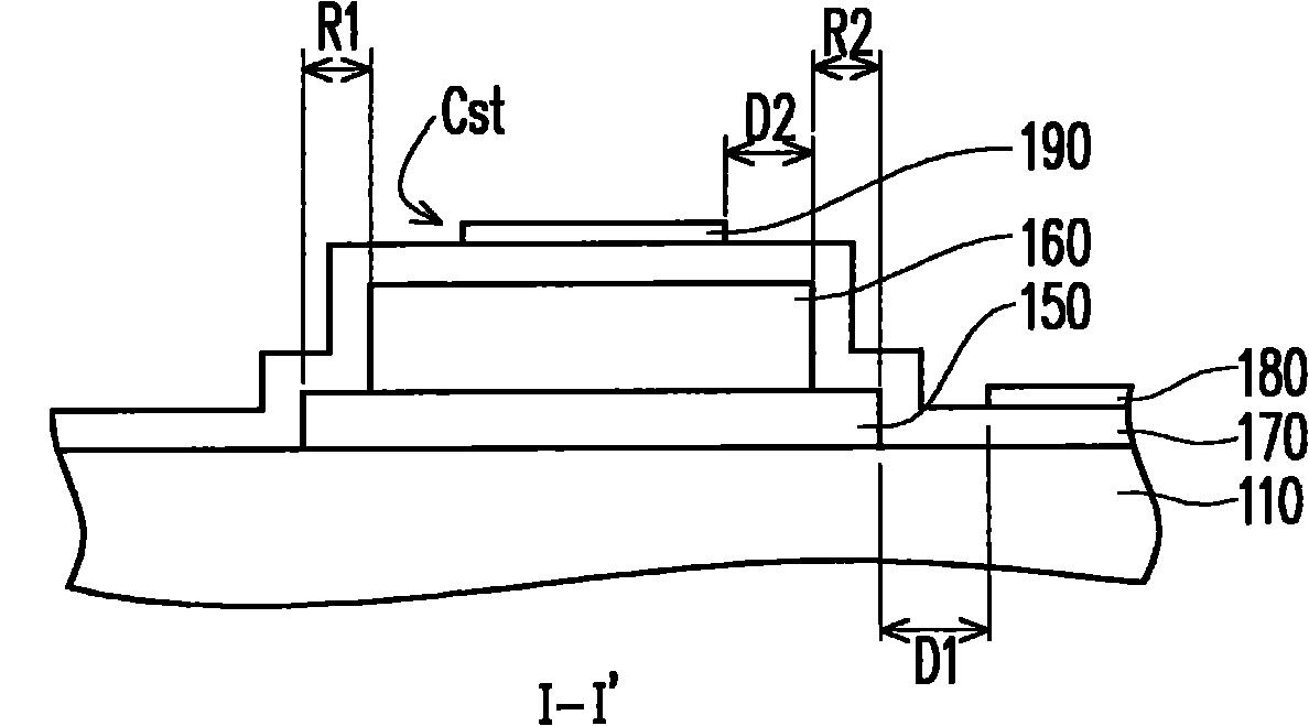
[0048] figure 1 A pixel structure according to an embodiment of the present invention is shown. figure 2 for figure 1 A partial cross-sectional view of the pixel structure. Please also refer to figure 1 and 2 The pixel structure 100 includes a substrate 110 , a scan line 120 , a data line 130 , a thin film transistor 140 , a semiconductor layer 150 , a metal capacitor electrode 160 , a protective layer 170 , a pixel electrode 180 and a transparent capacitor electrode 190 . In particular, the SMII storage capacitor Cst of this embodiment is composed of the semiconductor layer 150 , the metal capacitor electrode 160 , the protective layer 170 and the transparent capacitor electrode 190 .
[0049] In addition, the scan lines 120 and the data lines 130 are disposed on the substrate 110 , and...
PUM
 Abstract
Description
Claims
Application Information
 - R&D
- Intellectual Property
- Life Sciences
- Materials
- Tech Scout
- Unparalleled Data Quality
- Higher Quality Content
- 60% Fewer Hallucinations
Browse by: Latest US Patents, China's latest patents, Technical Efficacy Thesaurus, Application Domain, Technology Topic, Popular Technical Reports.
© 2025 PatSnap. All rights reserved.Legal|Privacy policy|Modern Slavery Act Transparency Statement|Sitemap|About US| Contact US: help@patsnap.com