Circuit board and processing method thereof

A processing method and circuit board technology, which is applied in the direction of assembling printed circuits with electrical components, printed circuits connected with non-printed electrical components, etc., can solve problems that limit product application and development, affect the electromagnetic performance of PCB products, and achieve guaranteed The effect of electromagnetic properties

Active Publication Date: 2013-04-10
SHENNAN CIRCUITS
View PDF6 Cites 0 Cited by
  • Summary
  • Abstract
  • Description
  • Claims
  • Application Information

AI Technical Summary

Problems solved by technology

Generally, the conductive coil on the PCB is set on the surface of the PCB. Therefore, when a large current is passed into the conductive coil, the conductive coil has a large loss in the air, which greatly affects the electromagnetic performance of the PCB product. The industry has continuously put forward higher requirements for current density. Therefore, the current design of conductive coils on PCBs cannot meet such requirements, which limits the application and development of products.

Method used


Image

  • Circuit board and processing method thereof
  • Circuit board and processing method thereof
  • Circuit board and processing method thereof

Examples


Embodiment Construction

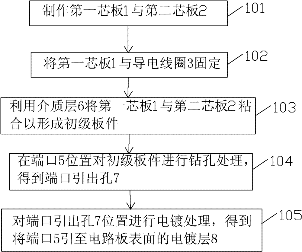
[0018] like figure 1 As shown, the embodiment of the present invention provides a circuit board processing method, which mainly includes:

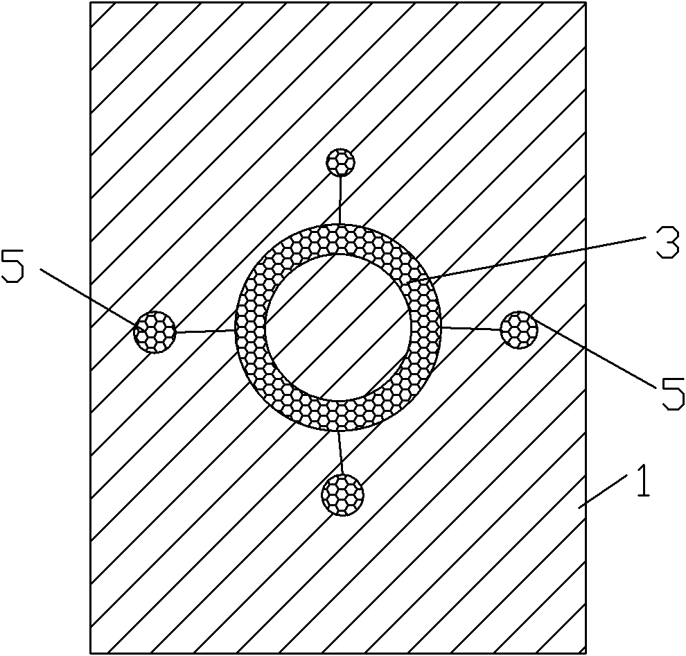
[0019] 101, first make the first core board 1 and the second core board 2, the first core board 1 or the second core board 2 can be formed by cladding copper on the base material (single-sided or double-sided), which can include two layers or multi-layer lines;

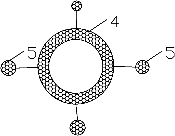
[0020] 102. Fix the first core board 1 and the conductive coil 3 with the port 5 in a certain way, and the conductive coil 3 can be as follows figure 2 As shown, it includes one or more turns of conductive wire 4 and port 5. The conductive wire 4 can be copper wire, gold wire, silver wire or aluminum wire, or it can be made of a mixture of various metals in copper, gold, silver and aluminum. Specifically, the conductive coil 3 can be welded to the first core board 1, and the conductive paste used for welding can be solder paste, copper paste or silver paste, etc., or the conduc...


PUM


Abstract

The embodiment of the invention relates to a circuit board processing method, comprising the following steps of: fixing a conductive coil on a first core board, arranging the conductive coil between the first core board and a second core board, and for leading the ports of the conductive coil out of the surface of the circuit board, drilling at the position of the ports, and electroplating at thepositions of port leading-out holes to obtain an electroplated layer for leading the ports out of the surface. The embodiment of the invention also provides a corresponding circuit board. Thus, the conductive coil is embedded in the circuit board and is not exposed on the surface of the circuit board, no loss is produced when current is introduced as the conductive coil is not exposed in the air,the electromagnetic properties of PCB (Printed Circuit Board) products are guaranteed, and especially the invention can be widely applied in the power supply industry with high requirement for current density.

Description

technical field [0001] The invention relates to the field of circuit boards, in particular to a circuit board processing method and a circuit board. Background technique [0002] The printed circuit board (PCB) is an important electronic component, a support for electronic components, and a provider of electrical connections for electronic components. Generally, the conductive coil on the PCB is set on the surface of the PCB. Therefore, when a large current is passed into the conductive coil, the conductive coil has a large loss in the air, which greatly affects the electromagnetic performance of the PCB product. The industry has continuously put forward higher requirements for current density. Therefore, the current design of the conductive coil on the PCB cannot meet such requirements, which limits the application and development of the product. Contents of the invention [0003] The technical problem to be solved by the embodiments of the present invention is to provid...

Claims


Application Information

Patent Timeline
Patent Type & Authority Patents(China)
IPC IPC(8): H05K3/32H05K1/18
Inventor 缪桦朱正涛彭勤卫孔令文
Owner SHENNAN CIRCUITS
Why Eureka
Try Eureka