Demodulation pixel with daisy chain charge storage sites and method of operation therefor

A charge storage and bit storage technology, which is applied to color TV parts, TV system parts, TVs, etc., can solve problems such as power consumption in pixels, and achieve the effect of reducing mismatching and mismatching problems

Active Publication Date: 2011-09-14
HEPTAGON MICRO OPTICS
View PDF4 Cites 6 Cited by
  • Summary
  • Abstract
  • Description
  • Claims
  • Application Information

AI Technical Summary

Problems solved by technology

Second, the electron current is used to generate a drift field, which results in significant in-pixel power dissipation

Method used


Image

  • Demodulation pixel with daisy chain charge storage sites and method of operation therefor
  • Demodulation pixel with daisy chain charge storage sites and method of operation therefor
  • Demodulation pixel with daisy chain charge storage sites and method of operation therefor

Examples


Embodiment Construction

[0039] The following discussion relates to sensors with p-doped substrates, where electrons are useful photo-generated charge carriers. All considerations can also be for n-doped materials, where holes are information carriers. In this case, the voltage applied to the gate and / or diffusion region will be reversed.

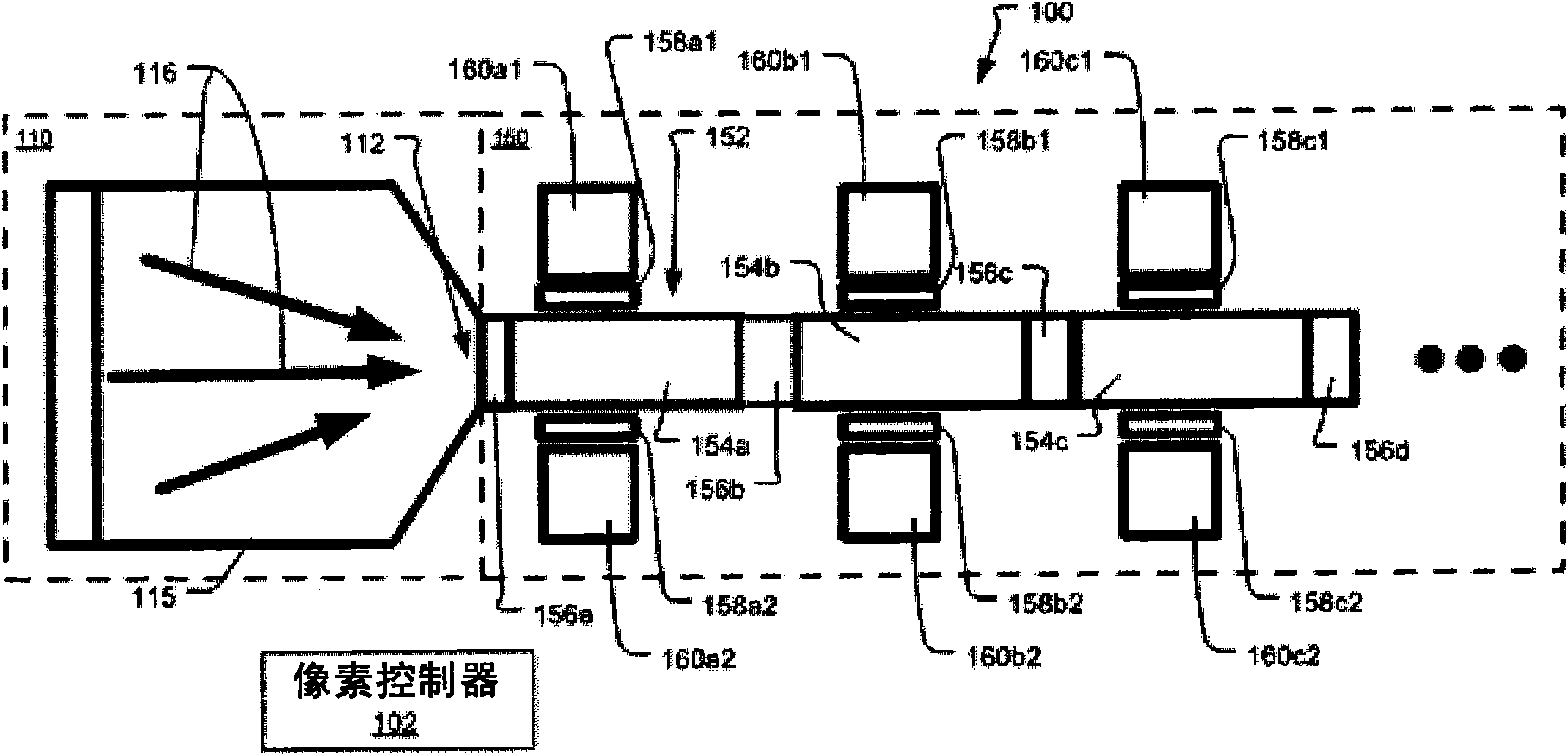
[0040] figure 1 A demodulation pixel 100 implemented in a semiconductor substrate is shown, which is constructed according to the principles of the present invention.

[0041] The pixel 100 includes a photosensitive area 110. Its typical feature is that a part of the semiconductor substrate receives incident light or other radiation and is not shielded by opaque layers such as materials and layers. The photosensitive area 110 has a photo-charge transfer area 115 that transfers the photo-charge to the pickup point 112, which is usually at one end of the transfer area 115.

[0042] Generally, the photocharge transfer area 115 transfers the photocharge to the pickup point...


PUM


Abstract

A demodulation pixel architecture allows for demodulating an incoming modulated electromagnetic wave, normally visible or infrared light. It is based on a charge coupled device (CCD) line connected to a drift field structure. The drift field is exposed to the incoming light. It collects the generated charge and forces it to move to the pick-up point. At this pick-up point, the CCD element samples the charge for a given time and then shifts the charge packets further on in the daisy chain. After a certain amount of shifts, the multiple charge packets are stored in so-called integration gates, in a preferred embodiment. The number of integration gates gives the number of simultaneously available taps. When the cycle is repeated several times, the charge is accumulated in the integration gates and thus the signal-to-noise ratio increases. The architecture is flexible in the number of taps. A dump node can be attached to the CCD line for dumping charge with the same speed as the samples are taken. Different implementations are described herein, which allow for smaller design or faster speed. The pixel structure can be exploited for e.g. 3D time-of-flight imaging. Both heterodyne and homodyne measurements are possible. Due to the highly-efficient charge transport enabled by static drift fields in the photo-sensitive region and small-sized gates in the CCD chain, high frequency bandwidth from just a few Hertz (Hz) up to greater GHz is supported. Thus, the pixel allows for highly-accurate optical distance measurements. Another possible application of this pixel architecture is fluorescence lifetime imaging microscopy (FLIM), where short laser pulses for triggering the fluorescence have to be suppressed.

Description

[0001] Related application [0002] This application claims the benefits of U.S. Provisional Patent Application No. 61 / 092,548 filed on August 28, 2008 under 35 USC 119(e), which is incorporated herein by reference in its entirety. [0003] Related application [0004] This application claims the benefits of U.S. Provisional Patent Application No. 61 / 092,548 filed on August 28, 2008 under 35 USC 119(e), which is incorporated herein by reference in its entirety. Background technique [0005] Demodulating the modulated light at the pixel level requires switching the photogenerated charge current. Although it is possible to deal with both electrons and hole currents, the current general method uses photogenerated electron currents. This choice was largely due to the higher electron mobility in semiconductor materials. Some pixel architectures perform the necessary signal processing based on photocurrent, while others work directly in charge domains. [0006] All pixel architectures tran...

Claims


Application Information

Patent Timeline
Patent Type & Authority Applications(China)
IPC IPC(8): H04N5/335H04N5/369H01L27/146G01S7/4914H04N5/372
CPCH01L27/14603H04N5/335G01S7/4914H04N5/369H01L27/14609H04N25/00H04N25/70
Inventor M·莱曼B·布艾特根
Owner HEPTAGON MICRO OPTICS
Why Eureka
Try Eureka