Packaging structure

An encapsulation structure and encapsulation colloid technology, applied in electrical components, electrical solid devices, circuits, etc., can solve the problems of increased circuit integration and complexity of the encapsulation structure, increased number of layers of circuit substrates, and limited circuit layout space. The effect of circuit layout design, reducing the number of layers, and saving production costs

Active Publication Date: 2011-09-21
ADVANCED SEMICON ENG INC
View PDF3 Cites 6 Cited by
  • Summary
  • Abstract
  • Description
  • Claims
  • Application Information

AI Technical Summary

Problems solved by technology

[0004] However, with the advancement of process technology, the circuit integration and complexity of the packaging structure are increasing day by day.
As far as the existing POP structure is concerned, based on its own structural characteristics, the space for line layout is severely limited, and the problem of mutual signal interference is also quite serious
On the other hand, due to the interleaving of the lines, the number of layers of the circuit substrate increases, and the signals of adjacent lines are also prone to mutual interference.
Although the use of multi-layer boards can increase the margin of circuit layout, it also relatively causes a burden on production costs.

Method used


Image

  • Packaging structure
  • Packaging structure
  • Packaging structure

Examples


Embodiment Construction

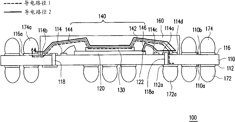
[0051] figure 1 A packaging structure according to an embodiment of the present invention is shown. Such as figure 1 As shown, the package structure 100 of this embodiment is suitable for package overlay technology, including a circuit substrate 110 , a chip 120 , a transfer interposer 130 , a plurality of bonding wires 140 , a plurality of solder balls 172 , 174 and an encapsulant 160 . The circuit substrate 110 has a bottom surface 110a and a top surface 110b opposite to each other. The chip 120 is disposed on the top surface 110 b of the circuit substrate 110 , and is electrically connected to the circuit substrate 110 by wire bonding technology.

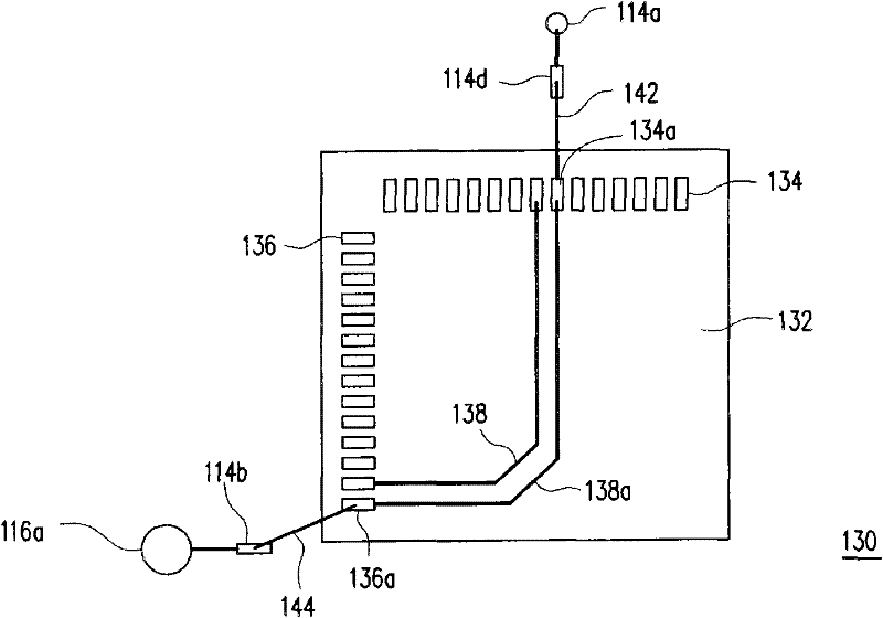
[0052] In addition, the circuit substrate 110 has a plurality of first bonding pads 112 on the bottom surface 110a, a plurality of bonding pads 114 and a plurality of second bonding pads 116 on the top surface 110b, wherein the second bonding pads 116 are arranged around the chip 120, And the bonding pad 114 is located between...


PUM


Abstract

The invention discloses a packaging structure which comprises a circuit substrate, a chip, a plurality of solder balls, a switch intermediate layer and packaging colloid. The circuit substrate is provided with a top surface and a bottom surface which are opposite to each other, and also provided with a plurality of first joints on the bottom surface and a plurality of second joints on the top surface. The chip is configured on the top surface of the circuit substrate and electrically connected to the circuit substrate. The plurality of solder balls are configured on part of the second joints respectively and enclose the chip. The switch intermediate layer is configured on the chip and electrically connected to the circuit substrate, wherein one joint in the first joints and the second joints is electrically connected to another joint in the first joints and the second joints through the switch intermediate layer. The packaging colloid is configured on the top surface of the circuit substrate, and at least covers the chip and the switch intermediate layer.

Description

technical field [0001] The present invention relates to a packaging structure, and in particular to a stacked packaging structure. Background technique [0002] System-in-package technology (SIP) is a technology that integrates two or more chips with independent functions into a single package. Faster development speed and lower development cost than system-on-chip (SoC). [0003] Package on Package (POP) process is a common assembly method in system-in-package technology, which stacks packaging units of chips with different functions, for example, stacking memory chip packaging units on logic chip packaging units. [0004] However, with the advancement of process technology, the circuit integration and complexity of the packaging structure are increasing day by day. As far as the existing POP structure is concerned, based on its own structural characteristics, the space for line layout is severely limited, and the problem of mutual signal interference is also quite seriou...

Claims


Application Information

Patent Timeline
Patent Type & Authority Applications(China)
IPC IPC(8): H01L23/482H01L23/49H01L25/00
CPCH01L2224/48227
Inventor 谢伯炘
Owner ADVANCED SEMICON ENG INC
Why Eureka
Try Eureka