Packaging structure of light-emitting diode emitting light in forward direction and formation method thereof

A light-emitting diode, forward light-emitting technology, applied in electrical components, electrical solid-state devices, circuits, etc., can solve the problems of rising product cost and product volume, and achieve the effect of increasing heat dissipation effect, improving luminous effect and life time.

Inactive Publication Date: 2011-09-21
ZHANJING TECH SHENZHEN +1
View PDF2 Cites 12 Cited by
  • Summary
  • Abstract
  • Description
  • Claims
  • Application Information

AI Technical Summary

Problems solved by technology

As a result, it will lead to the increase of p

Method used


Image

  • Packaging structure of light-emitting diode emitting light in forward direction and formation method thereof
  • Packaging structure of light-emitting diode emitting light in forward direction and formation method thereof
  • Packaging structure of light-emitting diode emitting light in forward direction and formation method thereof

Examples


Embodiment Construction

[0046]The packaging structure and method of forward-emitting light-emitting diodes provided by the present invention will be described in detail below in conjunction with illustrations and embodiments.

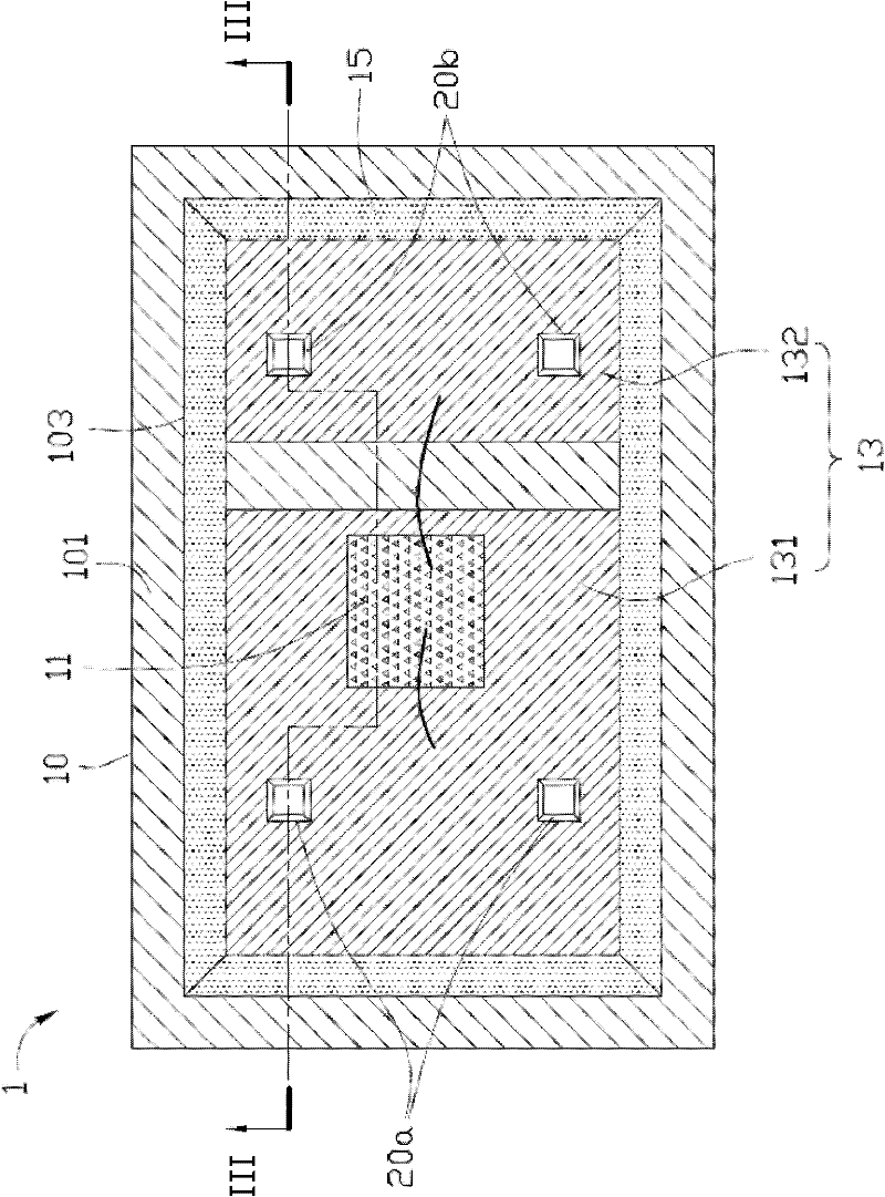
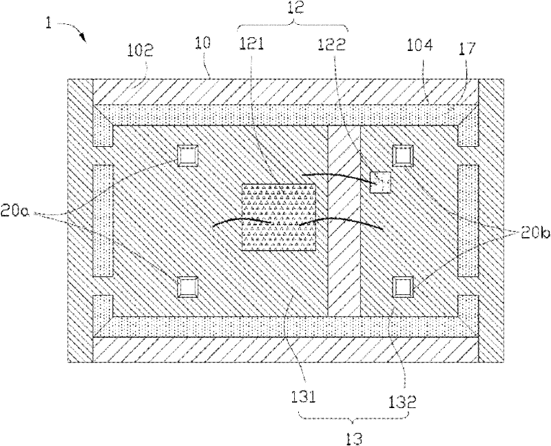
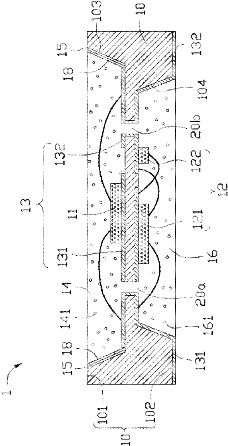
[0047] The first embodiment of the present invention provides a packaging structure 1 of a first forward-emitting semiconductor light-emitting component, please refer to Figure 1A , Figure 1B as well as Figure 1C . The package structure 1 of the above-mentioned first forward-emitting semiconductor light-emitting component includes a silicon substrate 10 , a first semiconductor component 11 , a second semiconductor component 12 and a circuit structure 13 . The above-mentioned silicon substrate 10 includes a first surface 101 and a second surface 102 , and the first surface 101 and the second surface 102 are respectively located on opposite sides of the silicon substrate 10 . The first surface 101 is the light-emitting surface of the packaging structure of the semiconductor...


PUM


Abstract

The invention provides a packaging structure of a light-emitting diode emitting light in a forward direction and a formation method thereof. The packaging structure of the light-emitting diode emitting light in the forward direction in two-sided light outgoing or single-side light outgoing is formed mainly through a two-sided circuit structure; and in addition, according to the invention, a silicon material is utilized as a semiconductor assembly packaging base plate, so as to enhance the heat dissipation effect of a semiconductor luminous assembly package, thus promoting the light-emitting effect and prolonging the service life.

Description

technical field [0001] The invention relates to a package structure of a semiconductor light-emitting component, in particular to a package structure of a forward-emitting light-emitting diode and a forming method thereof. Background technique [0002] With the advancement of semiconductor light emitting device technology, more and more products use light emitting diodes (light emitting diodes, LEDs), organic light emitting diodes (organic light emitting diodes, OLEDs) or lasers as light sources. Diodes (laser diodes, LDs). Compared with traditional light bulbs, the features of semiconductor light-emitting components include longer life, lower energy consumption, lower heat generation, less infrared light spectrum generation, and smaller component size (compact). However, the current industry's main requirement for the packaging structure of semiconductor light-emitting components is to form a surface mounted device (SMD) structure through the packaging structure, but the p...

Claims


Application Information

Patent Timeline
IPC IPC(8): H01L25/00H01L25/075H01L33/48H01L33/64H01L33/62
CPCH01L2224/48091H01L2224/48247H01L2224/73265H01L2924/00014
Inventor 谢明村曾文良陈隆欣林志勇
Owner ZHANJING TECH SHENZHEN
Why Eureka
Try Eureka