Controlling the recombination rate in a bipolar semiconductor component

A recombination rate, semiconductor technology, applied in the direction of semiconductor devices, electrical components, electronic switches, etc., can solve the problems of reducing the robustness of components, low on-resistance, etc.

Active Publication Date: 2011-09-21
INFINEON TECH AUSTRIA AG
View PDF6 Cites 10 Cited by
  • Summary
  • Abstract
  • Description
  • Claims
  • Application Information

AI Technical Summary

Problems solved by technology

A large number of charge carriers in the base region, i.e. a high-density charge-carrier plasma results in a low on-resistance of the component
However, the high plasma

Method used


Image

  • Controlling the recombination rate in a bipolar semiconductor component
  • Controlling the recombination rate in a bipolar semiconductor component
  • Controlling the recombination rate in a bipolar semiconductor component

Examples


Embodiment Construction

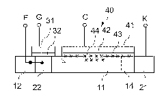
[0019] figure 1 A cross-sectional view of a bipolar semiconductor element is schematically illustrated, which in the present exemplary embodiment is realized as an IGBT. The component comprises a first base region 11 of the first conductivity type, a first emitter region 12 of the first conductivity type and a second emitter region 21 of the second conductivity type. The base region 11 is arranged between the first and the second emitter region 12 , 21 and has a lower doping concentration than the emitter region 12 , 21 . The doping concentration of the first and second emitter regions 12, 21 is, for example, 10 15 cm -3 and 10 21 cm -3 In the range in between, the second emitter region 21 may be doped lower than the first emitter region 12 . The doping concentration of the first base region 11 is, for example, 10 12 cm -3 and 10 15 cm -3 in the range between. The doping concentration of the first base region 11 and its size in the current flow direction of the compo...


PUM


Abstract

The invention relates to controlling the recombination rate in a bipolar semiconductor component. Disclosed is a method for controlling the recombination rate in the base region of a bipolar semiconductor component, and a bipolar semiconductor component.

Description

technical field [0001] Embodiments of the invention relate to bipolar semiconductor elements, and more particularly to controlling the rate of recombination in the base region of bipolar semiconductor elements. Background technique [0002] Bipolar components such as IGBTs, bipolar transistors, diodes or thyristors comprise two complementary doped emitters and at least one base region which is doped lower than the emitters and arranged between the emitters. [0003] In the on-state of the element, the two emitters emit charge carriers of different types, ie p-type and n-type charge carriers, forming a charge carrier plasma. A large number of charge carriers in the base region, ie a high density charge carrier plasma results in a low on-resistance of the component. However, high plasma density in the on-state results in high switching losses when the element is off. Also, high plasma density in the on-state may reduce the robustness of the component. [0004] There is ther...

Claims


Application Information

Patent Timeline
IPC IPC(8): H03K17/00H01L29/739H01L29/32
CPCH03K17/0412H01L29/739H01L29/861H01L29/0619H01L29/7397H01L29/7395H01L29/8611H01L29/0834H01L29/7393H01L29/408
Inventor F.希尔勒A.莫德F.D.普菲尔施H-J.舒尔茨
Owner INFINEON TECH AUSTRIA AG
Why Eureka
Try Eureka