LED epitaxial wafer and preparation method therefor

An LED epitaxial wafer and reaction chamber technology, applied in electrical components, circuits, semiconductor devices, etc., can solve the problems of low radiation recombination probability, low internal quantum efficiency, low luminous efficiency, etc., and achieve high hole concentration, high mobility, The effect of improving the injection efficiency

Inactive Publication Date: 2017-09-15
SOUTH CHINA NORMAL UNIVERSITY
View PDF1 Cites 9 Cited by
  • Summary
  • Abstract
  • Description
  • Claims
  • Application Information

AI Technical Summary

Problems solved by technology

[0004] The purpose of the present invention is to provide an LED epitaxial wafer to solve the problems of low luminous efficiency and low internal quantum effici

Method used


Image

  • LED epitaxial wafer and preparation method therefor
  • LED epitaxial wafer and preparation method therefor
  • LED epitaxial wafer and preparation method therefor

Examples


Embodiment 1

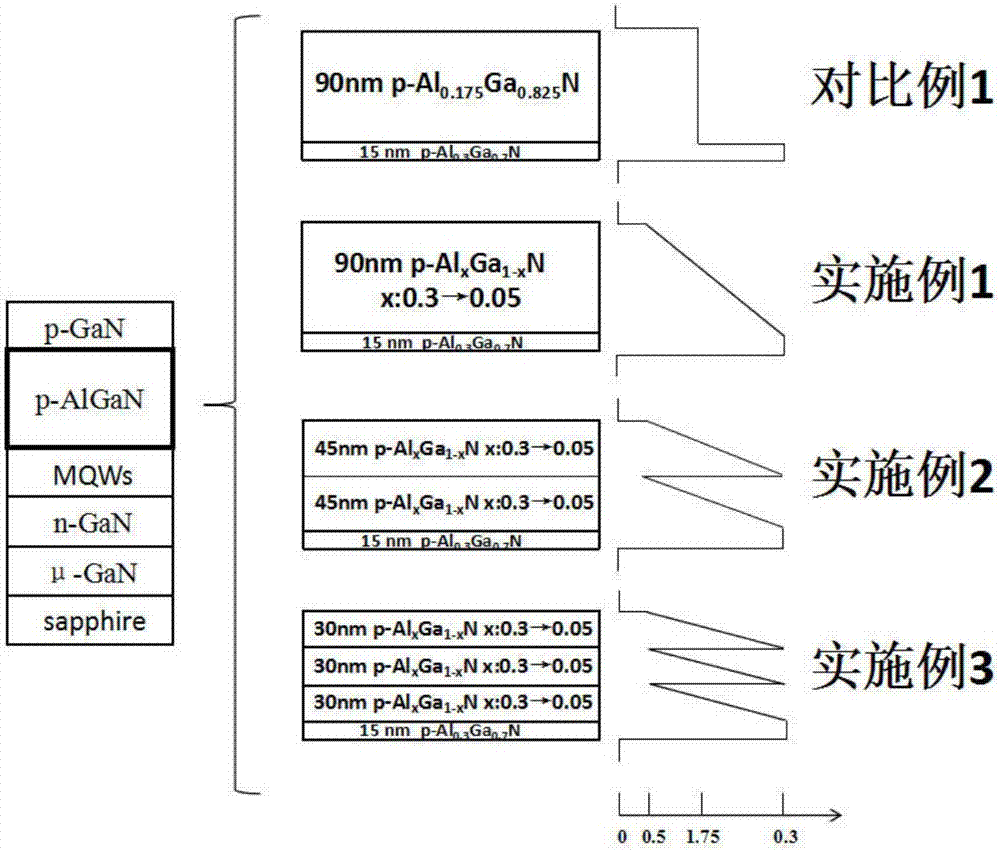
[0039] It is roughly the same as Comparative Example 1, except that the p-type layer of Comparative Example 1 is changed to p-type AlGaN whose Al composition is gradually reduced from 0.3 to 0.05 by using polarization-induced doping technology, and the thickness is also 90nm, and has Same average Al composition as Comparative Example 1.

Embodiment 2

[0041] It is substantially the same as Example 1, except that the p-type AlGaN layer whose Al composition is gradually changed from 0.3 to 0.05 in Example 1 is split into two 45nm p-type AlGaN polarization-induced doping graded layers, each The Al composition of the layers is gradually changed from 0.3 to 0.05, so the average Al composition is the same as that of the previous embodiment 1.

Embodiment 3

[0043] It is substantially the same as in Example 1, except that the p-type AlGaN layer whose Al composition is gradually changed from 0.3 to 0.05 in Example 1 is split into three 30nm p-type AlGaN polarization-induced doping graded layers, each The Al composition of the layers is gradually changed from 0.3 to 0.05, so the average Al composition is the same as that of the previous embodiment 1.

[0044] figure 1 It is a schematic structural diagram of the P-type layer of Examples 1-3 and Comparative Example 1.

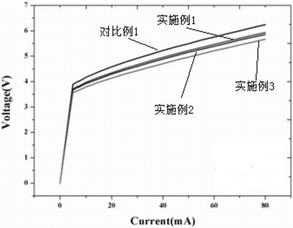
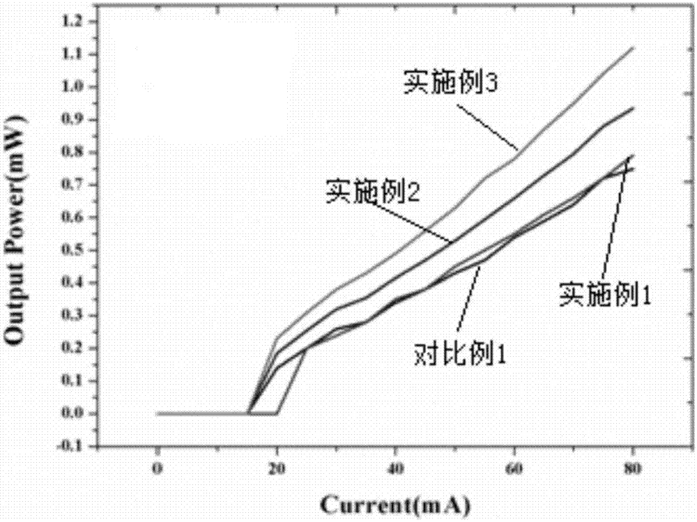
[0045] figure 2 It is the current-voltage curve diagram of three embodiments and Comparative Example 1. We can find that the forward voltage of Examples 1-3 is lower than that of Comparative Example 1. The results show that the forward voltage of the UV LED can be significantly reduced when the p-type layer is made by polarization-induced doping technology, which indicates that the p-type layer has lower resistivity than the ordinary p-type layer. And since the p-...


PUM

PropertyMeasurementUnit
Thicknessaaaaaaaaaa
Thicknessaaaaaaaaaa
Thicknessaaaaaaaaaa

Abstract

The invention relates to the preparation field of a photoelectric material, particularly to an LED epitaxial wafer. The LED epitaxial wafer comprises a substrate, a gallium nitride layer, an N type gallium nitride layer, an aluminum gallium nitride/gallium nitride multi-quantum-well layer, an electron barrier layer, a P type aluminum gallium nitride layer, a P type contact layer and a P type electrode which are arranged in an overlaying manner in sequence; and the P type aluminum gallium nitride layer is a Mg-doped multilayered polarization-induced Al<x>Ga<1-x>N layer, wherein x is 0.3 to 0.05. The invention aims to solve the technical problems of low luminous efficiency, low internal quantum efficiency and the like caused by electronic leakage and relatively low radiative recombination rate due to spontaneous and piezoelectric polarization in the LED; and the LED epitaxial wafer has the advantages of simple structure, simple and convenient process, convenience in production and suitability for industrial production.

Description

technical field [0001] The invention relates to the field of light-emitting diodes, in particular to an LED epitaxial wafer and a preparation method thereof. Background technique [0002] Since the 1990s, since ultraviolet light has great application value in various fields and industries, the focus of LED (light-emitting diode) research has gradually shifted to short-wavelength ultraviolet light. Among the many application fields of UV lamps, UV curing has the highest market share, accounting for about one-third of the UV lamp market, and more than 80% of the current UV LED market, and UV curing requires ultraviolet light around 365nm . UV curing is a process in which the liquid ultraviolet material converts the photoinitiator into free radicals or cations under the medium and short-wave radiation of ultraviolet light, so that the resin is polymerized into an insoluble and infusible solid coating film. It emerged in the 1960s A new technology was able to develop rapidly i...

Claims


Application Information

Patent Timeline
IPC IPC(8): H01L33/02H01L33/14H01L33/00
CPCH01L33/025H01L33/007H01L33/14
Inventor 肖稼凯李述体
Owner SOUTH CHINA NORMAL UNIVERSITY
Why Eureka
Try Eureka