Quantum detection element with low noise and method for manufacturing such a photodetection element

a detection element and detector technology, applied in the direction of sustainable manufacturing/processing, climate sustainability, semiconductor devices, etc., can solve the problems of reducing the absorption of detectors, reducing the thickness of space charge zones, and not revealing photodetection elements allowing a reduction of generation-recombination currents, etc., to reduce dark currents and reduce diffusion currents.

Active Publication Date: 2016-11-03
CENT NAT DE LA RECHERCHE SCI +1
View PDF0 Cites 9 Cited by
  • Summary
  • Abstract
  • Description
  • Claims
  • Application Information

AI Technical Summary

Benefits of technology

[0028]Advantageously, the resonance at the central wavelength of the spectral detection band is located in the layer of absorbent semi-conducting material, making it possible to limit the absorption at the surface and on the interfaces.
[0034]The thickness of the waveguide determines number of resonances in the guide. Advantageously, the thickness of the waveguide lies between λ0 / 8n and λ0 / n, advantageously between λ0 / 4n and 3λ0 / 4n, where n is the average value of the real parts of the refractive indices of the layers of semi-conducting material forming the waveguide. By choosing a sufficiently large thickness, one ensures that there is at least one resonance at the sought-after wavelength in the layer of absorbent semi-conducting material. By limiting the thickness, one limits the number of resonances in the layer of absorbent semi-conducting material, thereby making it possible to space the resonance wavelengths and to facilitate the occurrence of a “resonance node” at λrad.
[0035]According to a variant, the coupling grating or gratings comprise a periodic structure, of period lying between λ0 / n and λ0 / n1, where n1 is the real part of the refractive index of the medium of incidence of the radiation (for example air). These conditions on the period of the grating or gratings make it possible to limit the number of diffraction orders in the stack of layers forming the waveguide, more precisely to have only the diffraction order 0 in the incident medium and the diffracted orders 0, −1 and +1 in the waveguide, thereby once again making it possible to space the resonance wavelengths. This configuration moreover allows very good angular tolerance of the detection element.
[0038]Advantageously, the heterojunction comprises barrier layers, allowing a large reduction in the diffusion current.
[0039]According to a variant, at least one of the barrier layers is structured on at least one part of its thickness so as to form a grating for coupling with the optical cavity. The applicants have shown that this configuration made it possible to further reduce the dark current on account of the reduction in the active surface area.

Problems solved by technology

However, a decrease in the thickness of the space charge zone is also manifested by a decrease in the absorption of the detector.
None of these documents however discloses photodetection elements allowing a reduction in the generation-recombination current, in particular within junctions with low diffusion current.

Method used


Image

  • Quantum detection element with low noise and method for manufacturing such a photodetection element
  • Quantum detection element with low noise and method for manufacturing such a photodetection element
  • Quantum detection element with low noise and method for manufacturing such a photodetection element

Examples


Embodiment Construction

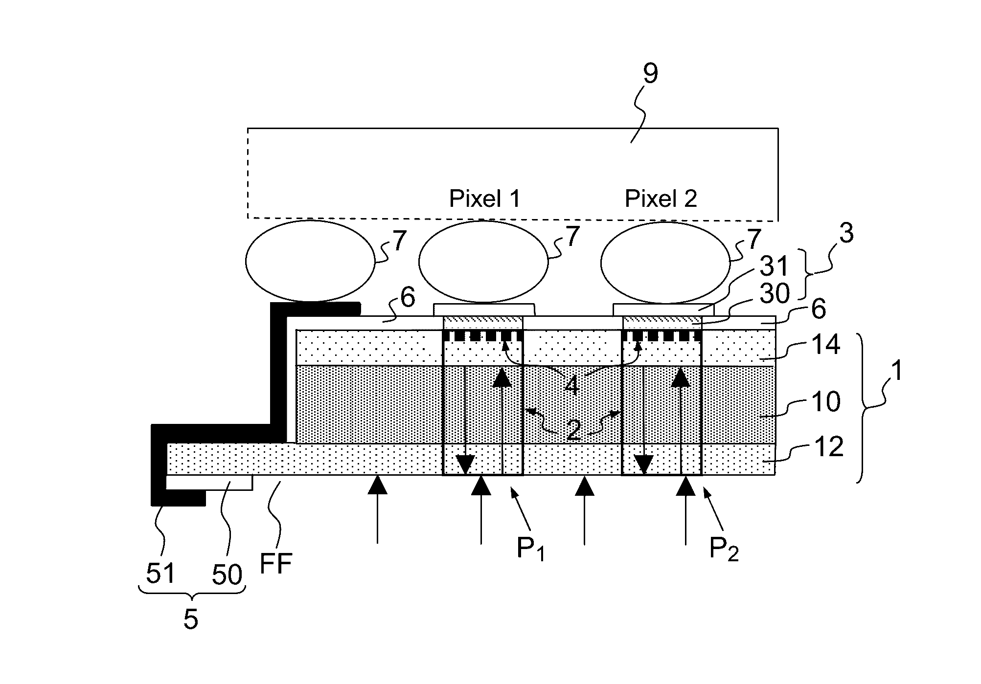
[0066]In the figures, identical elements are referenced by the same labels. The figures are given by way of illustration and are not necessarily to scale.

[0067]FIGS. 3A and 3B represent two examples of quantum detectors comprising quantum photodetection elements according to the present description.

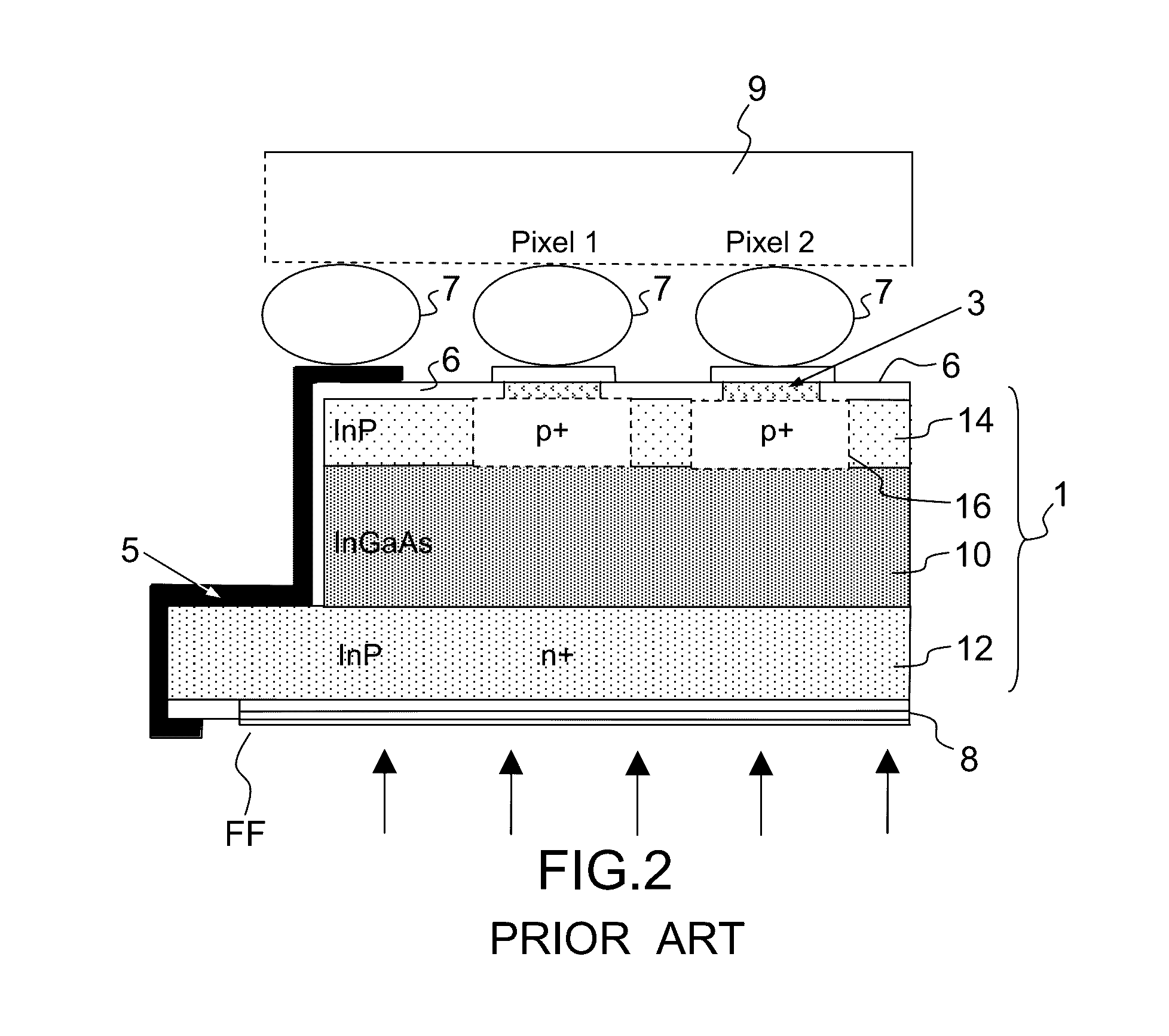
[0068]As in the example illustrated in FIG. 2, the detector comprises a set of photodetection elements (P1, P2, . . . ), for example arranged in a matrix manner in a focal plane of an imaging optic (not represented). In FIGS. 3A and 3B, the inter-pixel distance is overestimated for the sake of readability of the figures; The photodetection elements are suitable for the detection of an incident radiation in a spectral band centered around a central wavelength λ0, for example in one of the bands I, II or III of the infrared, corresponding to the spectral bands of atmospheric transparency. The detector comprises a front face FF intended to receive the luminous radiation indicated by arrows i...


PUM


Abstract

According to one aspect, the invention relates to an element for quantum photodetection of an incident radiation in a spectral band centred around a central wavelength λ0, having a front surface intended for receiving said radiation, and including: a stack of layers of semiconductor material forming a PN or PIN junction and including at least one layer made of an absorbent semiconductor material having a cut-off wavelength λ0>λ0, the stack of layers of semiconductor material forming a resonant optical cavity; and a structure for coupling the incident radiation with the optical cavity such as to form a resonance at the central wavelength λ0 allowing the absorption of more than 80% in the layer of absorbent semiconductor material at said central wavelength, and an absence of resonance at the radiative wavelength λrad, wherein the radiative wavelength λrad is the wavelength for which, at operating temperature, the radiative recombination rate is the highest.

Description

PRIOR ART[0001]1. Technical Field of the Invention[0002]The present invention relates to a quantum photodetection element with very low noise and to a method for manufacturing such a photodetection element. The invention applies notably to the design of photodetectors in the infrared having very good sensitivity.[0003]2. Prior Art[0004]An optical detector converts optical radiation into an electrical signal. This photon-electron conversion may be indirect: in the case of thermal detectors for example, the absorption of light is manifested by a temperature rise of an absorbent material which is thereafter converted into an electrical signal. Photonic (or quantum) detectors involve on the contrary the direct creation of electrical charge which may be either ejected (photoemissive effect) or released within the photosensitive material (case of semi-conducting materials).[0005]Photoresistors and photodiodes feature in particular among semi-conductor detectors. Photoresistors (or LDRs: L...

Claims


Application Information

Patent Timeline
Patent Type & Authority Applications(United States)
IPC IPC(8): H01L31/0232H01L31/0352H01L31/0304H01L31/109
CPCH01L31/02327H01L31/109H01L31/105H01L31/0304H01L31/03046H01L31/035209Y02P70/50Y02E10/544
Inventor PORTIER, BENJAMINVERDUN, MICHAELHAIDAR, RIADPELOUARD, JEAN-LUCPARDO, FABRICE
Owner CENT NAT DE LA RECHERCHE SCI
Why Eureka
Try Eureka