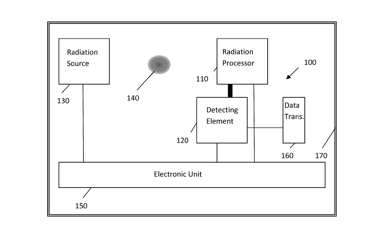
Implantable sensor

a sensor and sensor technology, applied in the field of implantable sensors, can solve the problems of limited absorption and diffraction of packaging

Active Publication Date: 2017-03-16
INDIGO DIABETES NV
View PDF0 Cites 12 Cited by
  • Summary
  • Abstract
  • Description
  • Claims
  • Application Information

AI Technical Summary

Benefits of technology

[0040]Frequency or time-domain multiplexing may be used for increasing a number of channels for spectrally processing radiation.
[0041]A Vernier-shifted spectral response may be used for increasing a number of channels for spectrally processing radiation.

Problems solved by technology

The shape of the sensor may allow small thickness of the biocompatible packaging, so that absorption and diffraction by the packaging can be limited.

Method used


Image

  • Implantable sensor
  • Implantable sensor
  • Implantable sensor

Examples


Embodiment Construction

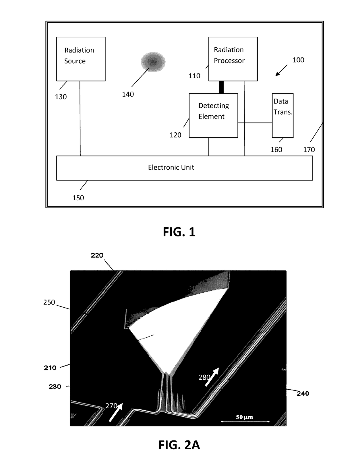
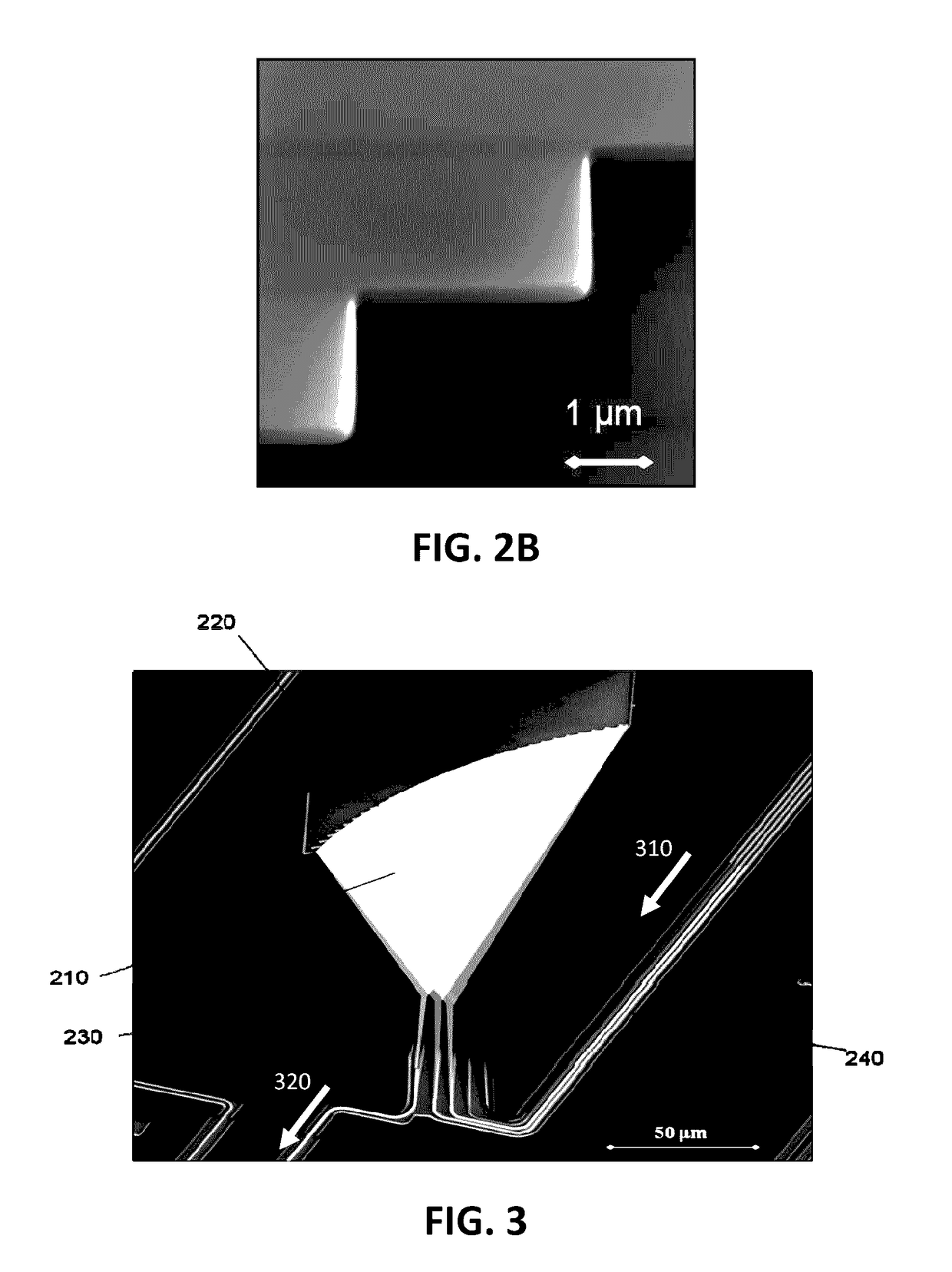
[0070]Where in embodiments of the present application reference is made to a photonics integrated circuit (PIC), this refers to a variety of forms and material systems such as for example low-index contrast waveguide platforms (e.g. polymer waveguides, glass / silica waveguides, AlxGa1-xAs waveguides, InxGa1-xAsyP1-y waveguides), high-index contrast waveguides (e.g. Silicon-on-Insulator, semiconductor membranes), plasmonic waveguides (e.g. metal nano-particle arrays, metal layers), also called Photonic Lightwave circuits (PLC). A photonic integrated circuit comprises at least one integrated optical component, such as for example but not limiting to an integrated optical cavity, an integrated optical resonator, an integrated optical interferometer, an integrated optical coupler, a waveguide, a taper, a tunable filter, a phase-shifter, a grating, a modulator, a detector, a source, a multiplexer, a demultiplexer or a combination thereof. The optical components can be active or passive. T...


PUM


Abstract

A sensor for sensing a substance such as for example glucose. The sensor is implantable in the body of a living creature. The sensor has a photonic integrated circuit, e.g. silicon-photonics integrated circuit, for spectrally processing radiation interacting with the sample. A continuous monitoring system can also include such a sensor.

Description

CROSS REFERENCE[0001]This application is a continuation-in-part application claiming benefit of U.S. patent application Ser. No. 13 / 415,392, filed Mar. 8, 2012, which is a continuation-in-part application claiming the benefit of international application PCT / EP2010 / 063263, filed Sep. 9, 2010, which claims the benefit of British application GB 0915775.1, filed Sep. 9, 2009, the entirety of said applications being incorporated herein by reference.FIELD[0002]The invention relates to the field of implantable sensors. More particularly, the present invention relates to implantable sensors for sensing substances and to corresponding continuous monitoring systems.BACKGROUND OF THE INVENTION[0003]According to the estimates of the World Health Organization (WHO), the number of people with diabetes will increase from 177 million in 2000 to 300 million by 2025. It is also estimated that 9% of all deaths worldwide are due to diabetes. Although diabetes is presently not curable, intensive insuli...

Claims


Application Information

Patent Timeline
Patent Type & Authority Applications(United States)
IPC IPC(8): A61B5/1455A61B5/145
CPCA61B5/1455A61B5/0066A61B5/14546A61B5/14532A61B5/0031A61B5/0075A61B5/1459A61B5/686A61B2562/028G01B9/02044G01B9/02051G01B9/02091G02B6/12021G02B6/34G02B2006/12061G02B2006/12107G02B2006/12123G02B2006/12138
Inventor DELBEKE, DANAEBAETS, ROELBOGAERTS, WIMRYCKEBOER, EVA MARIA PAULA
Owner INDIGO DIABETES NV
Why Eureka
Try Eureka