Method for preparing porous SOG film

a technology of porous sog and film, which is applied in the direction of chemical vapor deposition coating, plasma technique, coating, etc., can solve the problems of increasing the diameter of the holes present in the resulting porous film the relative dielectric constant of the resulting product is too large to reduce the relative dielectric constant, and the hygroscopicity of the resulting porous film is reduced. , the effect of reducing the hygroscopicity

Inactive Publication Date: 2005-07-19
ULVAC INC
View PDF12 Cites 13 Cited by
  • Summary
  • Abstract
  • Description
  • Claims
  • Application Information

AI Technical Summary

Benefits of technology

[0012]Moreover, the inventors of the present invention have also conducted various studies to inhibit any penetration of moisture such as water vapor through the surface of the porous SiO2 film prepared by the foregoing method and to control or reduce the hygroscopicity of the porous film. As a result, the inventors of this invention have succeeded in the preparation of a porous SiO2 film having a low relative dielectric constant or an interlayer insulating film consisting of a hydrophobic porous SiO2 film by forming a porous SiO2 film while adding a surfactant to the reaction system containing an organic silane, and then repeating this step at least one time to further form a porous SiO2 film on the porous film formed in the previous step and to thus give a multi-layered SiO2 film; or inserting a specific hydrophobic film between every neighboring two porous films; or capping or coating the surface of the porous film with a specific hydrophobic film, and have found that the resulting porous film or the interlayer insulating film never causes any change in the relative dielectric constant even when an additional film or films are further deposited on the porous film in the semiconductor device-fabricating process subsequent to the formation of the porous film. Thus, the inventors have accomplished the second object of the present invention.
[0013]The method for preparing a porous SOG film according to the second invention comprises the step of repeating, at least one time, the foregoing first step for preparing a porous SiO2 film to thus form in order a porous SiO2 film on the porous film formed in the first step. If a number of porous films are laminated in this way to give a multi-layered porous film, the hygroscopicity of the resulting porous SiO2 film is reduced and the relative dielectric constant thereof never causes any change even when a film is further deposited on or laminated with the porous film in the subsequent semiconductor device-fabricating process. As a result of such lamination, the porous films constituting the laminate are put in layers while the holes present in every neighboring porous films and arranged perpendicularly to the substrate deviate from one another and therefore, the holes present in the uppermost film have almost no communication with those present in the lowermost film or there is almost no through hole in the multi-layered film. The moisture absorption of the laminated porous film is thus controlled.
[0014]In the present invention, it is also possible to conduct the second step in which either of a SiO2 film, a SiNx film and a SiOxNy film is formed on the porous SiO2 film prepared in the foregoing first step by the CVD or sputtering method to thus cap the surface of the porous film; or to further repeat the foregoing first and second steps at least one time. In both of the monolayered porous film capped with a hydrophobic film in this way and the multilayered porous film, the moisture penetration and the hygroscopicity thereof are further reduced and controlled as compared with the porous film free of any cap of a hydrophobic film and the relative dielectric constant thereof is never changed even when an additional film is deposited thereon in the subsequent semiconductor device-fabricating process.
[0016]The method for preparing a porous SOG film according to the third invention comprises the steps of preparing an organic silane solution containing an organic silane, water and an alcohol, subjecting the organic silane to acid hydrolysis or alkaline hydrolysis, heat-treating the reaction system in the presence of a surfactant to give a porous SiO2 film and then subjecting the resulting porous SiO2 film to either of the treatment with oxygen plasma, the electron beam-irradiation treatment or the UV light-irradiation treatment, to thus remove the unreacted OH groups remaining in the porous SiO2 film. The following reaction occurs due to the foregoing treatments and thus the OH groups are removed:(OSiOH)2O→2SiO2+H2OThe residual OH groups are removed as H2O according to the foregoing reaction and the moisture in the atmosphere is thus never adsorbed on the porous film. Accordingly, the foregoing method can provide a porous film having a low relative dielectric constant and this in turn leads to the reduction of any corrosion of interconnections of, for instance, Al. In addition, this hydrophobic porous SiO2 film never causes any change in the relative dielectric constant even when an additional film or films are deposited thereon or laminated with the same in the subsequent semiconductor device-fabricating process.

Problems solved by technology

However, it is difficult to effectively reduce the interconnecting delay by simply using the interconnection of, for instance, Cu.
If a SiO2 film is formed according to the conventional technique and then a film is further deposited on the SiO2 film in the semiconductor device-fabricating process such as the CVD process, a problem arises, such that the relative dielectric constant of the resulting product increases.
In the case of the porous SiO2 film formed using an inorganic SOG, a problem arises such that the diameter of the holes present in the resulting porous film is too large to reduce the relative dielectric constant thereof by the formation of fine pores.
In addition, in the case of the SiO2 film formed using an organic silane, problems arise such that the resulting film is insufficient in the film quality and that the heat-resistant temperature thereof is low (not more than 450° C.).
Moreover, it has been known that the porous film formed by the foregoing conventional method absorbs moisture since the film has hygroscopicity due to the porous characteristics thereof and this in turn leads to corrosion of interconnections of, for instance, Al.
Moreover, even in the method for preparing a porous SOG film (or an interlayer insulating film) having a low relative dielectric constant, whose dielectric constant never causes any change when depositing another film on the interlayer insulating film according to, for instance, the CVD process after the formation of the interlayer insulating film, the penetration of moisture such as water vapor through the surface of the resulting porous SiO2 film often becomes a cause of a critical problem, since the holes present therein are arranged perpendicularly to the substrate.
Further, the inorganic SOG film includes a large quantity of OH groups and therefore, unreacted OH groups may still remain in the film even after the firing of the same.
Accordingly, a problem arises such that the moisture in the atmosphere is adsorbed on the film through the residual OH groups and this results in the corrosion of the Al interconnections.
Moreover, the foregoing chemical processing suffers from a problem of the difficulty in the control of the process.

Method used


Image

  • Method for preparing porous SOG film
  • Method for preparing porous SOG film
  • Method for preparing porous SOG film

Examples


example 1

The First Invention

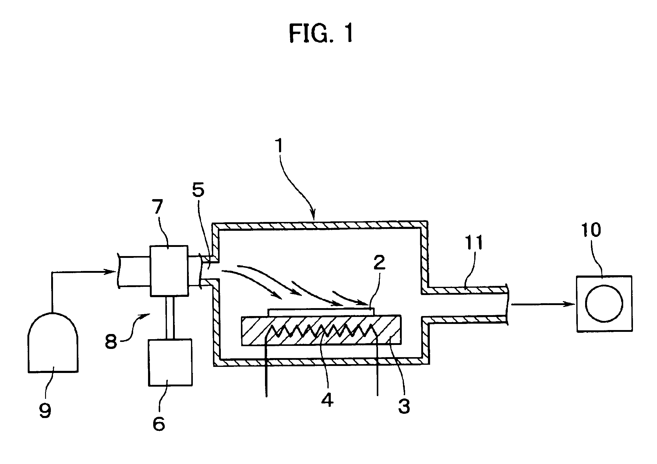
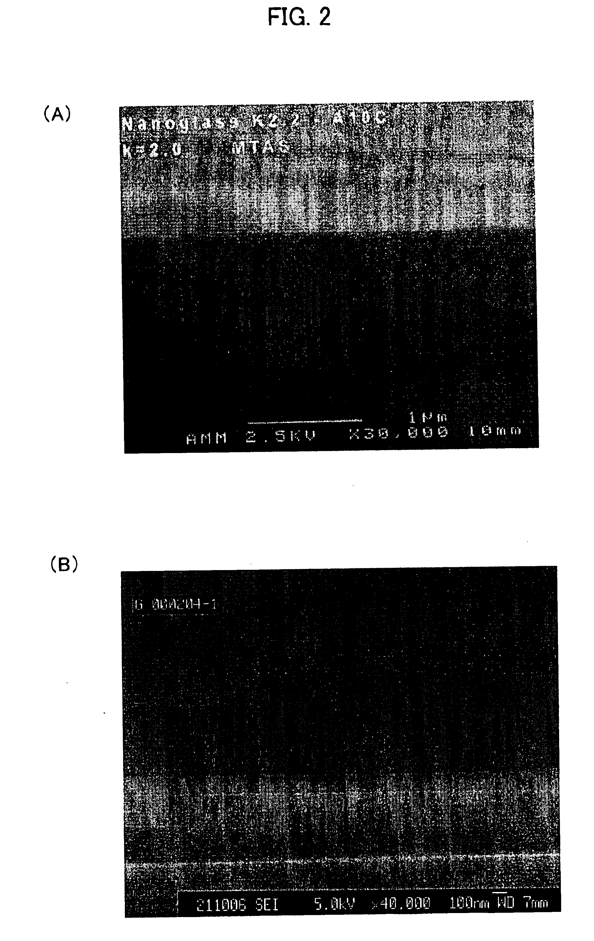
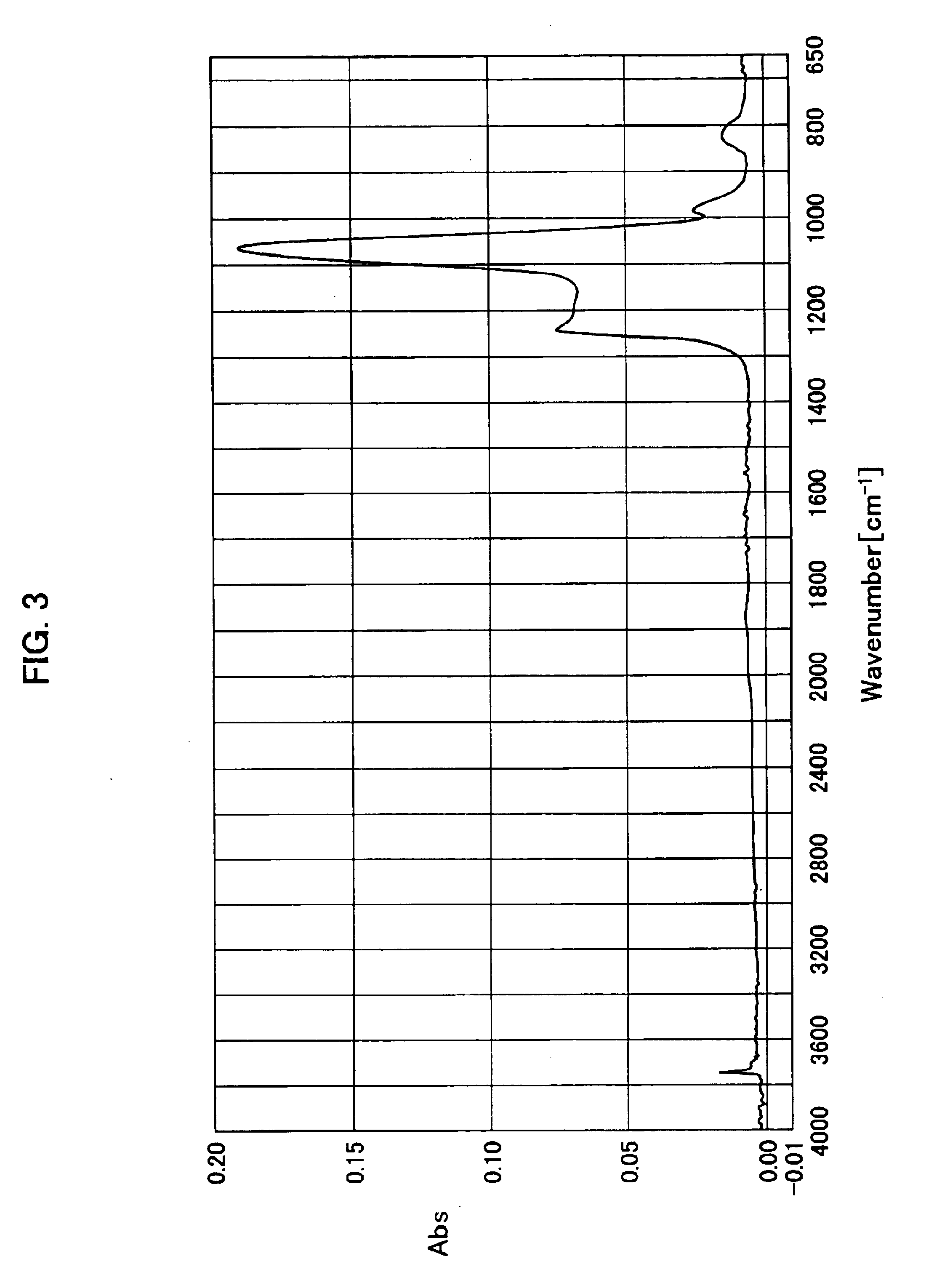
[0060]A SiO2 solution for forming a porous SiO2 film (or a SOG porous film) was prepared using, as starting materials, 0.7 mole of nitric acid, 12 moles of water, 15 moles of ethanol and a predetermined amount of a surfactant per one mole of TEOS. The surfactant used herein was n-hexadecyl trimethyl ammonium chloride (available from Kanto Chemical Co., Ltd. under the trade name of CTAC1) and this was used in an amount of 0.1, 0.15, 0.2 or 0.25 mole per mole of TEOS to thus give each coating solution. Each coating solution was applied onto the surface of a semiconductor substrate (Sample Nos. A1 to H1) under the condition of 3000 rpm using a spin coater. Using a known infrared heating furnace, each substrate provided with the coated layer was first treated at temperatures ranging from 200 to 400° C. in the air and then fired at a temperature of 400° C. in an atmosphere of 100 to 10−5 Pa, as indicated in the following Table 1, to thus form each corresponding porous ...

example 2

The Second Invention

[0066]An insulating film (Sample Nos. A2 to H2) consisting of a bilayer porous film was prepared by forming a porous film (thickness: 0.5 μm) according to the film-forming steps used in Example 1 and then forming a porous SiO2 film (thickness: 0.5 μm) similar to the foregoing porous film on the surface of the foregoing porous film by repeating the film-forming steps.

[0067]Aluminum was vapor-deposited on the multilayered porous SiO2 films thus prepared to form electrodes. After one week, the relative dielectric constants thereof were determined using a relative dielectric constant-measuring equipment available from HP Company (RF IMPEDANCE ANALYZER 4191A). The results thus obtained are listed in the following Table 2.

[0068]

TABLE 2Initial Heat-Second Heat-DielectricSampleTreatmentTreatmentSurfactant / TEOSConst.No.(° C.)(° C.)(molar ratio)(ε / ε0)A22004000.1 2.9B22004000.152.5C22004000.2 1.9D22004000.251.5E22504000.251.8F23004000.252.3G23504000.252.8H24004000.253.4

[006...

example 3

The Second Invention

[0072]A SiO2 film, a SiNx film or a SiOxNy film (thickness: 50 nm) was formed on the surface of the porous SiO2 film (thickness: 0.5 μm) obtained in the first step of Example 2 by the CVD or sputtering method to thus cap the surface of the porous film. Then the foregoing first step and the capping layer-forming step were repeated under the same conditions to thus form, in order, a porous film and a capping layer on the first capping layer.

[0073]Aluminum electrodes were vapor-deposited on the multilayered porous films thus prepared and thereafter the relative dielectric constants thereof were determined using a relative dielectric constant-measuring equipment available from HP Company (RF IMPEDANCE ANALYZER 4191A). As a result, it was found that values similar to those listed in Table 2 were obtained. Accordingly, such a multilayered porous film may be used as useful interlayer insulating film.


PUM

PropertyMeasurementUnit
temperaturesaaaaaaaaaa
heat-resistant temperatureaaaaaaaaaa

Abstract

A porous SOG film is formed by preparing an organic silane solution containing an organic silane, water and an alcohol, subjecting the organic silane to acid hydrolysis or alkali hydrolysis and then heat-treating the resulting reaction system in the presence of a surfactant to thus form a porous SiO2 film to use for an interlayer insulating film. Alternatively, a porous SOG film is formed by repeating the foregoing step at least one time; or by forming a hydrophobic film on the porous SiO2 film prepared by the foregoing step by the CVD or sputtering technique to thus cap the surface of the porous film; or repeating the porous film-forming and capping steps at least one time. Moreover, after the preparation of the foregoing porous SiO2 film, it is subjected to either of the oxygen plasma-treatment, electron beam-irradiation treatment and UV light-irradiation treatment to remove the unreacted OH groups remaining on the porous film and to thus form a porous SOG film. Further, the foregoing heat-treatment is carried out in the following two stages: in the first stage, the porous film is treated at a temperature capable of mainly removing the water and the alcohol through evaporation thereof; and in the second stage, the porous SiO2 film is treated at a temperature (350 to 450° C.) sufficient for covering at least the inner walls of the holes with the hydrophobic moieties of the surfactant.

Description

TECHNICAL FIELD[0001]The present invention relates to a method for preparing a porous SOG film and in particular to a method for preparing a porous SOG film, which comprises the steps of subjecting an organic silane to hydrolysis and then heat-treating the hydrolyzed organic silane in the presence of a surfactant.BACKGROUND ART[0002]Recently, distributing wires or interconnections of, for instance, copper (Cu) or aluminum (Al) have been adopted in the field of LSI and simultaneously, there have widely been conducted researches in and development of the interconnection structure and interlayer insulating films. However, it is difficult to effectively reduce the interconnecting delay by simply using the interconnection of, for instance, Cu. For this reason, in the semiconductor device-fabricating process, an oxide film (such as a SiO2 film) having a low relative dielectric constant is used as an interlayer insulating film and there has been proposed such an idea that the oxide film is...

Claims


Application Information

Patent Timeline
Patent Type & Authority Patents(United States)
IPC IPC(8): H01L21/02H01L21/768H01L21/70H01L21/316
CPCH01L21/02126H01L21/02203H01L21/02216H01L21/02282H01L21/0234H01L21/02359H01L21/02362H01L21/31695H01L21/7682H01L2221/1047
Inventor MURAKAMI, HIROHIKOTANAKA, CHIAKIHIRAKAWA, MASAAKI
Owner ULVAC INC
Why Eureka
Try Eureka