Wireless communication small card embedding device and manufacturing method thereof

A small card and embedded device technology, which is applied in semiconductor/solid-state device manufacturing, electrical components, circuits, etc., can solve the problems of capital investment barriers, inability to greatly improve material utilization, and inability to use IC cards, etc., to achieve satisfactory efficiency and low processing costs Low cost and material saving effect

Inactive Publication Date: 2011-09-28
SHANGHAI LIANZHENGYUAN ELECTROMECHANICAL TECH
View PDF3 Cites 6 Cited by
  • Summary
  • Abstract
  • Description
  • Claims
  • Application Information

AI Technical Summary

Problems solved by technology

Shenzhen Jinguanwei's dual-module packaging machine is only equipped with an additional set of packaging components on the previous standard IC card packaging machine, realizing the packaging of 2 IC card modules on a standard card, which only improves the packaging efficiency, but does not greatly improve the packaging efficiency. The utilization rate of materials, and the subsequent process can only write data to one IC modul

Method used


Image

  • Wireless communication small card embedding device and manufacturing method thereof
  • Wireless communication small card embedding device and manufacturing method thereof
  • Wireless communication small card embedding device and manufacturing method thereof

Examples


Embodiment

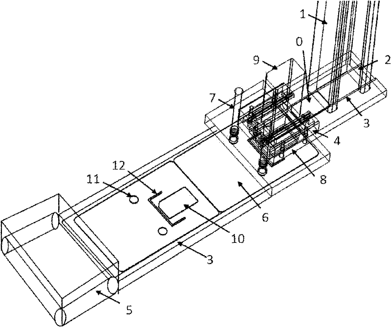
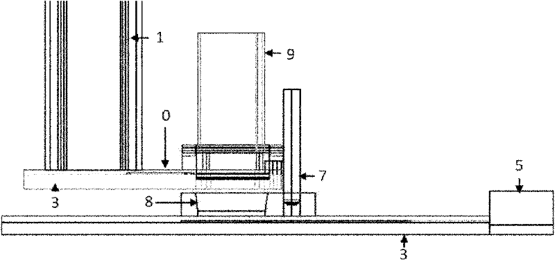
[0033] like figure 1 and figure 2 As shown, the wireless communication small card embedding device involved in this embodiment includes: small card stacking mechanism 1, unloading mechanism 2, transmission mechanism 3, embedding mechanism 4, material receiving mechanism 5 and card tray 6, wherein: small card The stacking mechanism 1, the embedding mechanism 4 and the receiving mechanism 5 are sequentially connected in series. The unloading mechanism 2 is located at the lower part of the small card stacking mechanism 1 and is connected with the small card stacking mechanism 1. The transmission mechanism 3 is connected with the unloading mechanism 2 respectively. , the embedding mechanism 4 is connected with the receiving mechanism 5, the card tray 6 is located at the junction of the transmission mechanism 3 and the embedding mechanism 4 and is used to embed the miniaturized SIM card 0, and the card tray embedded in the miniaturized SIM card 0 passes through the transmission me...


PUM

PropertyMeasurementUnit
Groove widthaaaaaaaaaa
Diameteraaaaaaaaaa

Abstract

The invention discloses a wireless communication small card embedding device and a manufacturing method thereof in the technical field of mobile communication. The device comprises a small card stacking mechanism, a blanking mechanism, a transmission mechanism, an embedding mechanism, a material receipt mechanism and a card support, wherein the small card stacking mechanism, the embedding mechanism and the material receipt mechanism are connected in series in turn; the blanking mechanism is positioned on the lower part of the small card stacking mechanism and is connected with the small card stacking mechanism; the transmission mechanism is connected with the blanking mechanism, the embedding mechanism and the material receipt mechanism respectively; and the card support is positioned at a combined position of the transmission mechanism and the embedding mechanism and is used for embedding a small subscriber identity module (SIM) card. Characteristics of original equipment are not influenced at all, and a standard integrated circuit (IC) intelligent card can be produced according to an original production process through reasonable process configuration. Flexible switching can be performed between the standard card production process and the small SIM card production process by the device, so that the utilization rate of polyvinyl chloride (PVC) materials is improved by 5 to 10 times under the condition that the equipment is not modified on a large scale.

Description

technical field [0001] The present invention relates to a device and method in the technical field of mobile communication, in particular to a small wireless communication card embedding device and a manufacturing method thereof. Background technique [0002] As the environmental concept of low-carbon emission reduction is becoming more and more popular, various industries are taking various measures in their respective fields to reduce the consumption of materials and energy in the production process of products. In the field of mobile communications, China Mobile has begun to implement a miniaturized SIM card plan, and gradually tends to purchase miniaturized SIM cards instead of large SIM cards similar to the size of business cards. Most of the mobile phones currently on the market only support miniaturized SIM cards, not card trays. In the past, large SIM cards were produced to be compatible with older mobile phones. Therefore, direct production of miniaturized SIM car...

Claims


Application Information

Patent Timeline
IPC IPC(8): H01L21/00H01L21/50
Inventor 莫华强
Owner SHANGHAI LIANZHENGYUAN ELECTROMECHANICAL TECH
Why Eureka
Try Eureka