Photonic device and manufacturing method thereof

A technology of optoelectronic devices and light-emitting devices, which is applied in semiconductor/solid-state device manufacturing, circuits, electrical components, etc., can solve the problems of different aging rates and difficulty in achieving uniformity, and achieve the goal of improving uniformity, prolonging usable life, and reducing size Effect

Active Publication Date: 2013-07-24
EPISTAR CORP
View PDF1 Cites 0 Cited by
  • Summary
  • Abstract
  • Description
  • Claims
  • Application Information

AI Technical Summary

Problems solved by technology

Good uniformity is difficult to achieve due to manufacturing factors and aging of the LEDs, where each LED may age at a different rate

Method used


Image

  • Photonic device and manufacturing method thereof
  • Photonic device and manufacturing method thereof
  • Photonic device and manufacturing method thereof

Examples


Embodiment Construction

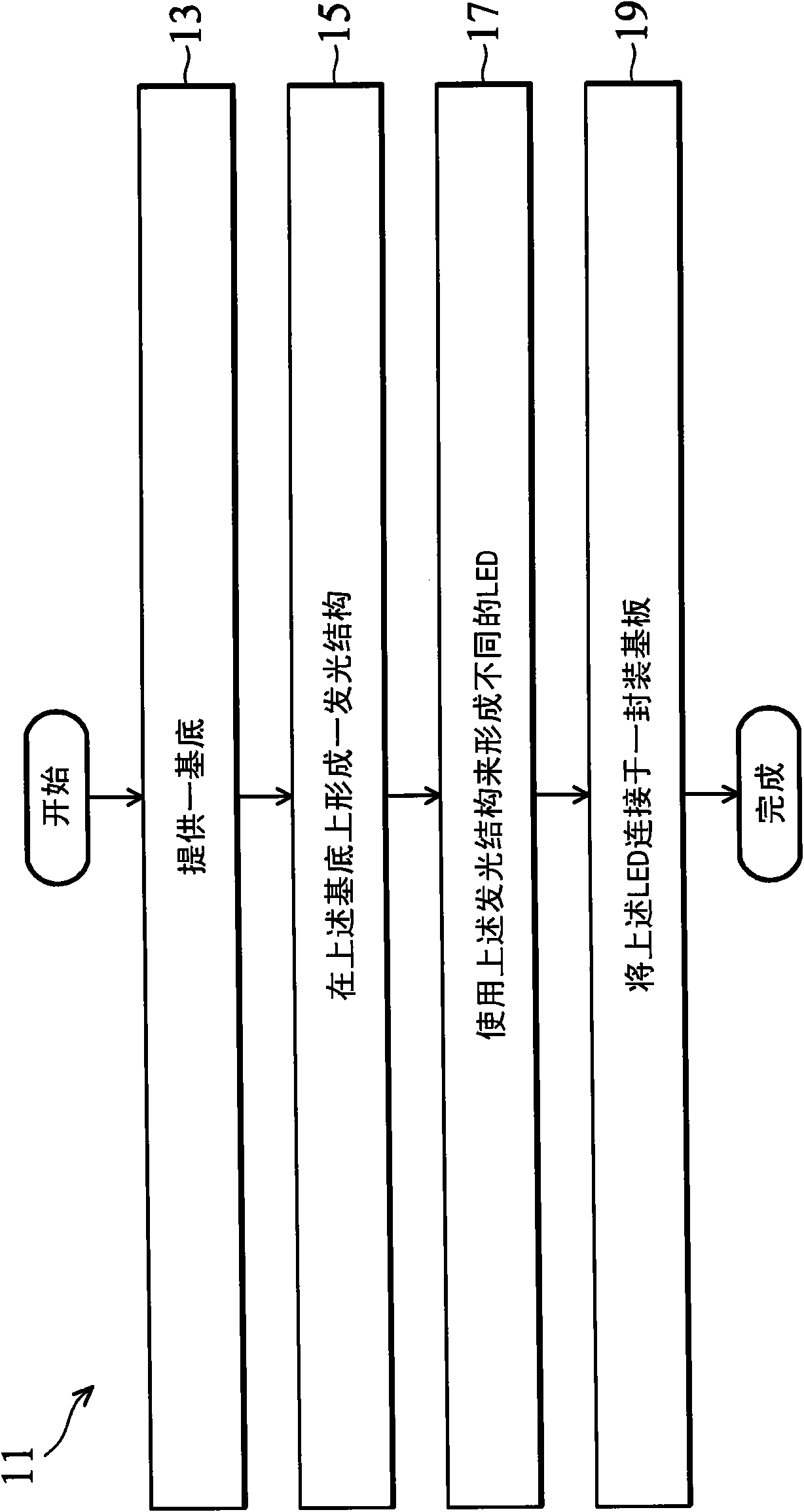
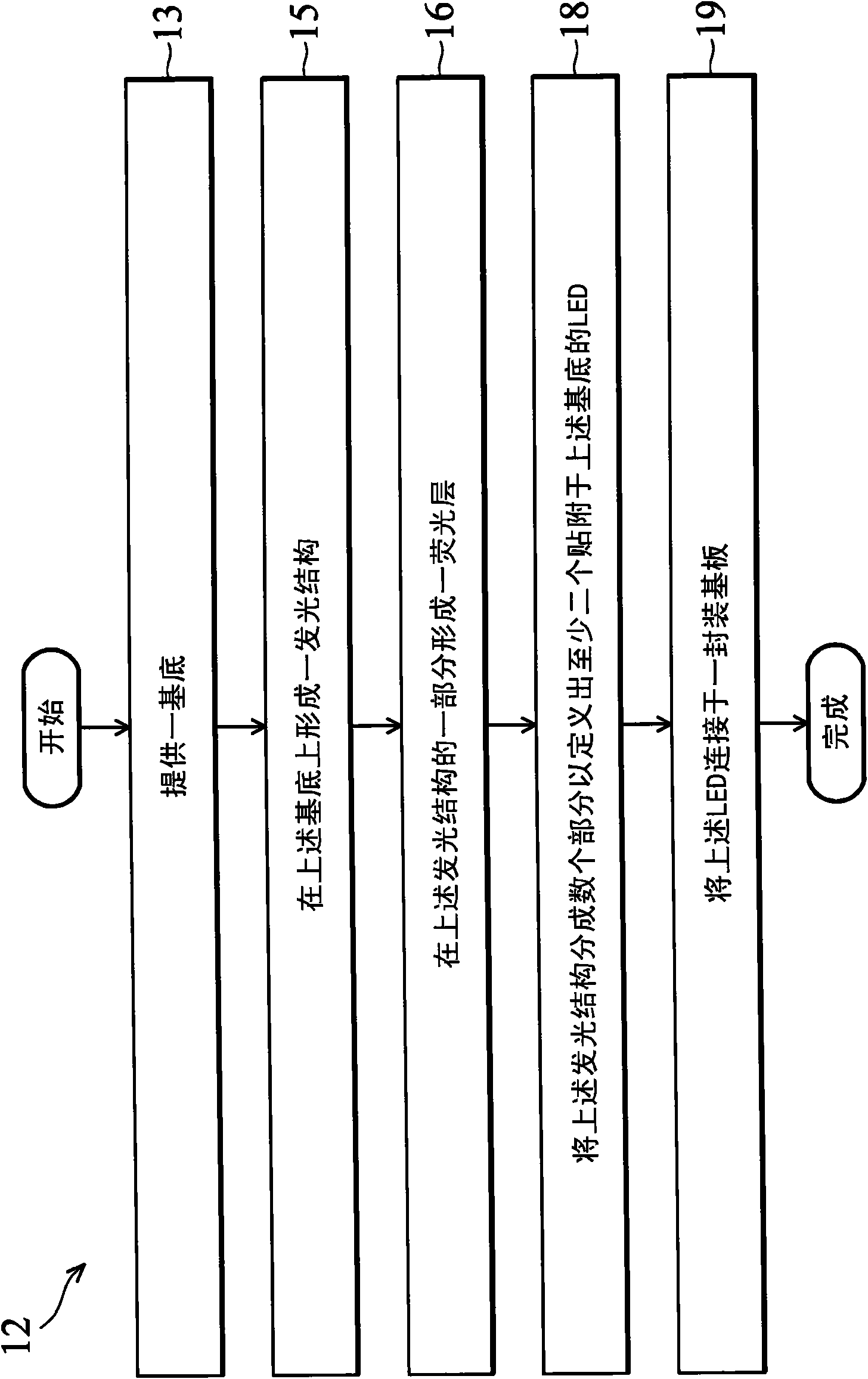
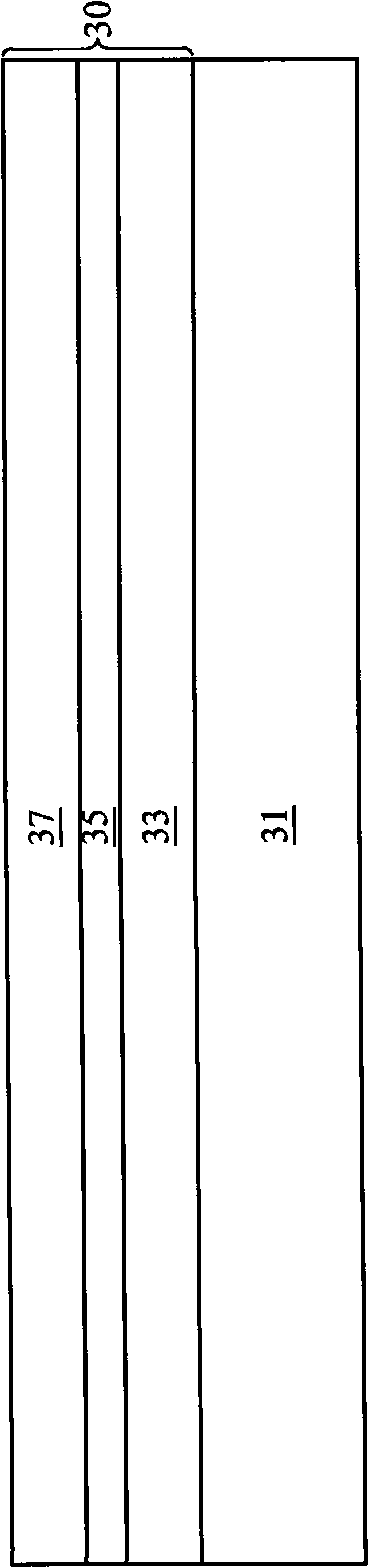
[0044] In order to make the above-mentioned and other objects, features, and advantages of the present invention more comprehensible, the preferred embodiments are specifically listed below, together with the accompanying drawings, and are described in detail as follows:

[0045] It is to be appreciated that the following disclosure of this specification provides many different embodiments, or examples, for implementing the various features of the invention. However, the following disclosures in this specification describe specific examples of each component and its arrangement in order to simplify the description of the invention. Of course, these specific examples are not intended to limit the present invention. For example, if the following disclosure in this specification describes that a first feature is formed on or above a first feature, it means that it includes the embodiment in which the above-mentioned first feature and the above-mentioned second feature are formed ...


PUM


Abstract

A photonic device generates light from a full spectrum of lights including white light. The device includes two or more LEDs grown on a substrate, each generating light of a different wavelength and separately controlled. A light-emitting structure is formed on the substrate and apportioned into the two or more LEDs by etching to separate the light-emitting structure into different portions. At least one of the LEDs is coated with a phosphor material so that different wavelengths of light are generated by the LEDs while the same wavelength of light is emitted from the light-emitting structure.

Description

technical field [0001] The present invention relates to semiconductor devices and manufacturing methods thereof, and more particularly to integrated optoelectronic devices. Background technique [0002] A light-emitting device (LED)—as used herein, is a semiconductor light source having a light-emitting diode and optional photoluminescence material—also referred to herein as a fluorescent material—to emit Light of a specific wavelength or range of wavelengths. LEDs are traditionally used for lighting fixtures, but there is an increasing trend for displays. An LED emits light when a voltage is applied across a p-n junction formed by layers of semiconductor material having opposite characteristics of dopants. Different materials can be used to emit light of different wavelengths by changing the bandgap of the semiconductor layer and creating an active layer in the above-mentioned P-N junction. The voltage applied above controls the intensity of the light. In addition, the ...

Claims


Application Information

Patent Timeline
Patent Type & Authority Patents(China)
IPC IPC(8): H01L27/15H01L21/782H01L33/48
CPCH01L27/153H01L33/382H01L33/0079H01L33/508H01L33/504H01L2224/48091H01L2924/13091H01L2924/1305H01L2224/45147H01L2224/45144H01L33/0093H01L2924/00014H01L2924/00H01L33/502H01L33/62
Inventor 黄信杰王昭雄
Owner EPISTAR CORP
Why Eureka
Try Eureka