Semiconductor-device driving circuit, and semiconductor apparatus having the same
A technology for driving circuits and semiconductors, which is used in semiconductor devices, output power conversion devices, circuits, etc.
- Summary
- Abstract
- Description
- Claims
- Application Information
AI Technical Summary
Problems solved by technology
Method used
Image
Examples
Embodiment approach 1
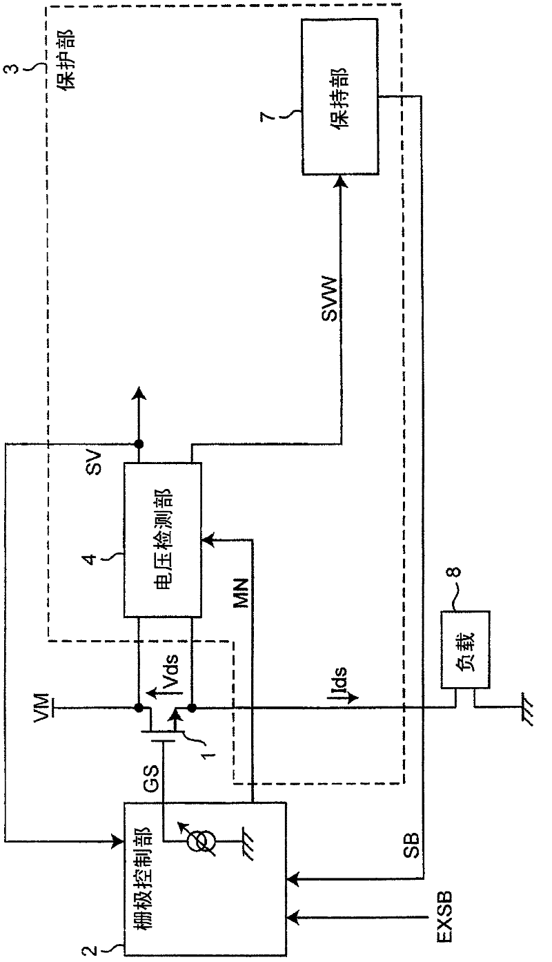
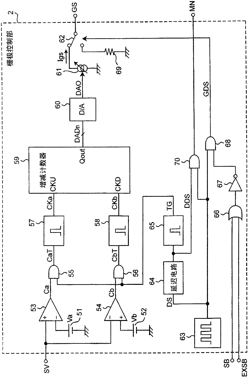
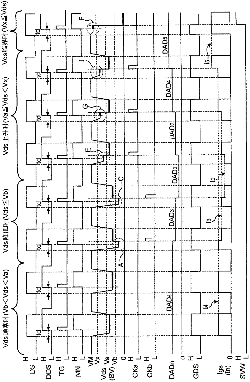
[0081] figure 1 It is a block diagram showing a drive circuit according to Embodiment 1 of the present invention and a circuit configuration of a semiconductor device including the drive circuit. exist figure 1 Among them, the switching element 1 that is a semiconductor element that is driven and controlled by the driving circuit of the first embodiment is an FET using a p-type region for a gate. Here, the "FET using a p-type region for the gate" is a FET composed of a semiconductor stacked structure, a p-type semiconductor layer is in contact with the semiconductor stacked structure, and the p-type semiconductor layer is used as the gate electrode. the FET. In addition, in the semiconductor multilayer structure, although the portion in contact with the p-type semiconductor layer is undoped, it may be n-type or p-type. The semiconductor stacked structure in Embodiment 1 is, for example, a nitride semiconductor.
[0082] In the switching element 1 of the drive circuit acc...
Embodiment approach 2
[0125] Figure 5 It is a block diagram showing a drive circuit according to Embodiment 2 of the present invention and a circuit configuration of a semiconductor device including the drive circuit. In addition, in Embodiment 2, the switching element 1, which is a semiconductor element driven and controlled by the drive circuit, is described using a FET using a p-type region for the gate, but using a Schottky electrode for the gate It is self-evident that the same effect can be achieved in FETs and other semiconductor elements. In the following description of Embodiment 2, elements having the same functions and configurations as those in the driving circuit and semiconductor device of Embodiment 1 described above are assigned the same reference numerals, and description thereof will be omitted.
[0126] exist Figure 5 In FIG. 1 , a gate control unit 12 as a gate control unit is connected to the gate of the switching element 1 using a p-type region FET as the gate. In additio...
Embodiment approach 3
[0154] Figure 9 It is a block diagram showing a drive circuit according to Embodiment 3 of the present invention and a circuit configuration of a semiconductor device including the drive circuit. Also in Embodiment 3, the switching element 1 which is a semiconductor element which is driven and controlled by a drive circuit is described using a FET using a p-type region for the gate, but the switching element 1 using a Schottky electrode for the gate It is self-evident that the same effect can be obtained in FET and other semiconductor elements. In the following description of Embodiment 3, elements having the same functions and configurations as those in the driving circuit and semiconductor device of Embodiments 1 and 2 described above are assigned the same reference numerals, and description thereof will be omitted.
[0155] In the drive circuit of Embodiment 3, the voltage detection unit 4 in the drive circuit of Embodiment 1 and the current detection unit 5 in Embodiment...
PUM
 Abstract
Description
Claims
Application Information
 - R&D
- Intellectual Property
- Life Sciences
- Materials
- Tech Scout
- Unparalleled Data Quality
- Higher Quality Content
- 60% Fewer Hallucinations
Browse by: Latest US Patents, China's latest patents, Technical Efficacy Thesaurus, Application Domain, Technology Topic, Popular Technical Reports.
© 2025 PatSnap. All rights reserved.Legal|Privacy policy|Modern Slavery Act Transparency Statement|Sitemap|About US| Contact US: help@patsnap.com


