Method for preparing local oxidization termination ring of semiconductor device

A local oxidation and semiconductor technology, which is applied in the manufacture of semiconductor/solid-state devices, electrical components, circuits, etc., can solve the problems of insufficient thickness, affecting the breakdown performance of semiconductor high-voltage devices, etc., and achieve the effect of improving breakdown performance

Active Publication Date: 2011-10-05
SHANGHAI HUAHONG GRACE SEMICON MFG CORP
View PDF3 Cites 6 Cited by
  • Summary
  • Abstract
  • Description
  • Claims
  • Application Information

AI Technical Summary

Problems solved by technology

Termination rings in the prior art are usually formed by local oxidation, however, the thickness of the field oxide layer (Field Oxide, FOX) formed by the local oxidation method in the prior art is insufficient, thus affecting the breakdown performance of semiconductor high-voltage devices

Method used


Image

  • Method for preparing local oxidization termination ring of semiconductor device
  • Method for preparing local oxidization termination ring of semiconductor device
  • Method for preparing local oxidization termination ring of semiconductor device

Examples


Embodiment Construction

[0020] In order to make the object, technical solution and advantages of the present invention clearer, the present invention will be further described in detail below in conjunction with the accompanying drawings.

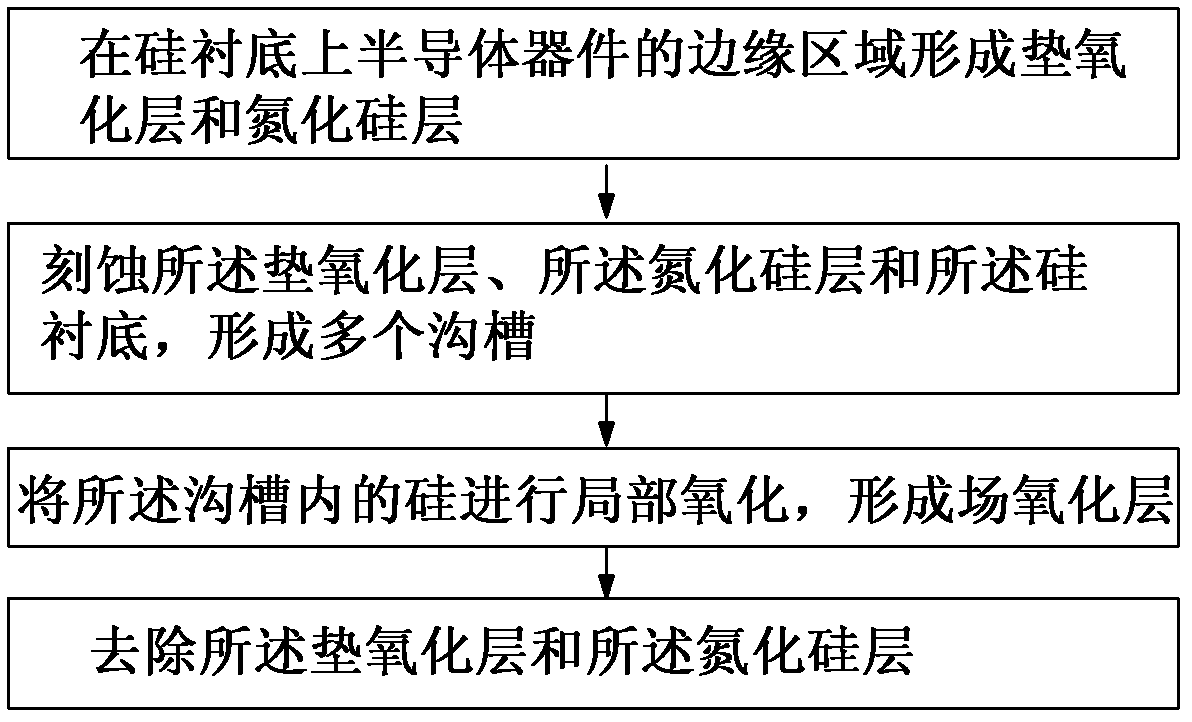
[0021] see figure 1 , figure 1 It is a flow chart of the preparation method of the partial oxidation termination ring of the semiconductor device of the present invention. Preferably, the method for preparing a partial oxidation termination ring of a semiconductor device of the present invention is a preparation method for a partial oxidation termination ring of a deep semiconductor device, and is used in a high-voltage semiconductor device. The preparation method of the partial oxidation termination ring of the semiconductor device of the present invention comprises the following steps:

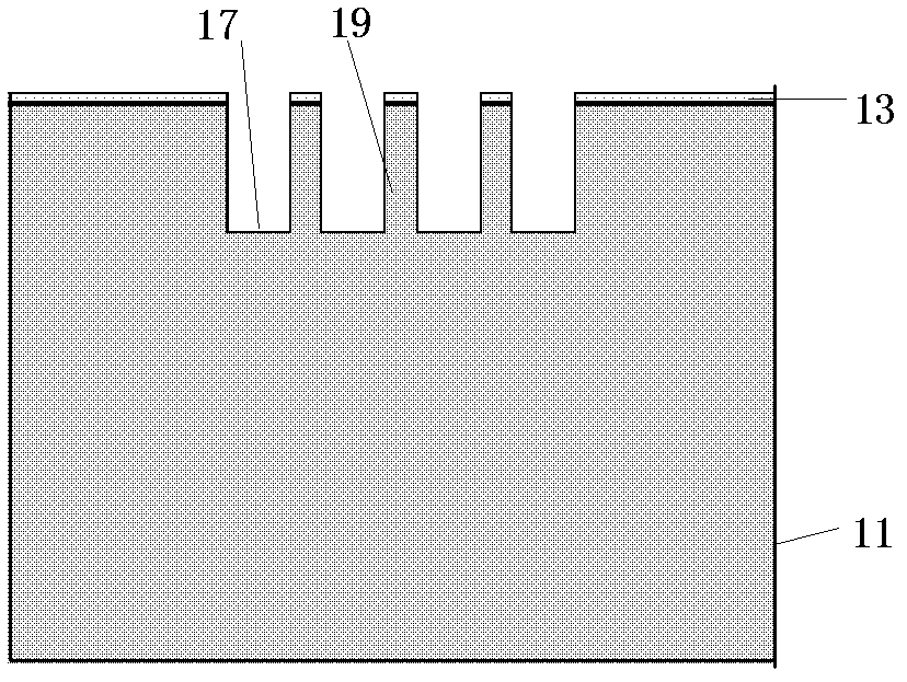
[0022] A pad oxide layer and a silicon nitride layer are formed at an edge region of a semiconductor device on a silicon substrate. The pad oxide layer is used to protect the...


PUM


Abstract

The invention relates to a method for preparing a local oxidization termination ring of a semiconductor device, which comprises the following steps of: forming a pad oxide layer and a silicon nitride layer in an edge zone of the semiconductor device on a silicon substrate; etching the pad oxide layer, the silicon nitride layer and the silicon substrate to form a plurality of grooves; carrying out local oxidation on silicon in the grooves to form a field oxide layer; and removing the pad oxide layer and the silicon nitride layer. The local oxide termination ring of the semiconductor device, which is prepared by adopting the method, has high breakdown voltage and can well improve the breakdown property of the semiconductor device.

Description

technical field [0001] The invention relates to a method for preparing a local oxidation termination ring (LOCOS Termination) of a semiconductor device, in particular to a preparation method for a deep layer (Buried) local oxidation termination ring of a high-voltage semiconductor device. Background technique [0002] In the manufacturing process of modern semiconductor devices, the breakdown resistance (Breakdown) performance of semiconductor devices is more and more expected by people. In order to improve the breakdown voltage (Breakdown Voltage, BV) of the semiconductor device, the semiconductor device has a termination ring (Termination) structure, which surrounds the active area of ​​the semiconductor device, so as to prevent the edge part of the semiconductor device from being broken down early. Termination rings in the prior art are usually formed by local oxidation. However, the thickness of the Field Oxide (FOX) layer formed by the local oxidation method in the prio...

Claims


Application Information

Patent Timeline
Patent Type & Authority Applications(China)
IPC IPC(8): H01L21/02H01L21/316
Inventor 王颢
Owner SHANGHAI HUAHONG GRACE SEMICON MFG CORP
Why Eureka
Try Eureka