

Scale-span design method for interface structure of micro/nano/photoelectronic device
A technology of optoelectronic devices and interface structures, which is applied in the fields of instruments, computing, and electrical digital data processing, etc., can solve the problems of insufficient, increased computing time, huge time, etc., and achieve the effect of high efficiency and solving design problems
- Summary
- Abstract
- Description
- Claims
- Application Information
AI Technical Summary
Problems solved by technology
Method used
Image

Examples
Embodiment
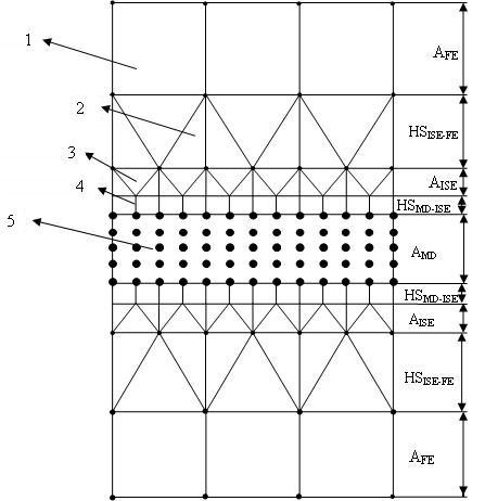
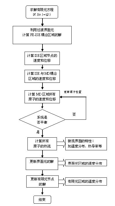
[0028] at a thickness of 2 umThe temperature boundary conditions of -500K and 500K were applied to both ends of the Cu thin film respectively. According to the flow chart of cross-scale design, firstly, in the FE Area (FE Area, A FE ), use the finite element method to discretize it and solve its stiffness matrix and load array, and impose the upper and lower temperature boundary conditions: -500K, 500K, which is the second step in the above specific implementation steps; secondly, use the transition Interface element method, the results of the finite element solution are linked with the interface element, and the solution of the interface element area is calculated; then, the obtained solution is applied to the interface area (ISE Area, A ISE ), and use it as the initial condition of the non-equilibrium molecular dynamics simulation in the molecular dynamics model to solve the calculation, which is the third step in the above specific implementation steps; after the solution...
PUM
 Abstract
Description
Claims
Application Information