Grid-control metal-insulator device based on electronic tunneling

A quantum tunneling and insulator layer technology, which is applied in semiconductor devices, semiconductor/solid-state device manufacturing, electrical components, etc., can solve problems such as high reaction probability, and achieve the effect of improving performance and reducing leakage current flow.

Inactive Publication Date: 2013-07-10
FUDAN UNIV
View PDF3 Cites 0 Cited by
  • Summary
  • Abstract
  • Description
  • Claims
  • Application Information

AI Technical Summary

Problems solved by technology

Those whose energy is higher than the potential barrier and whose motion direction is suitable may not necessarily react, it can only be said that the probability of reaction is relatively high

Method used


Image

  • Grid-control metal-insulator device based on electronic tunneling
  • Grid-control metal-insulator device based on electronic tunneling
  • Grid-control metal-insulator device based on electronic tunneling

Examples


Embodiment Construction

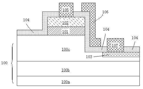
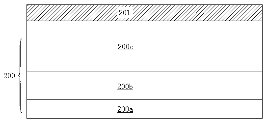
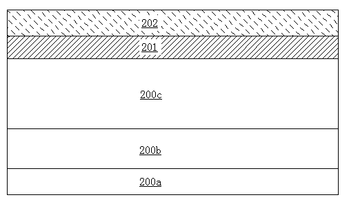
[0033] An exemplary embodiment of the present invention will be described in detail below with reference to the accompanying drawings. In the drawings, the thicknesses of layers and regions are enlarged or reduced for convenience of description, and the shown sizes do not represent actual sizes. Although these figures do not fully reflect the actual size of the device, they still completely reflect the mutual positions between the regions and the constituent structures, especially the upper-lower and adjacent relationships between the constituent structures. The representations in the referenced figures are schematic, but this should not be considered as limiting the scope of the invention. Meanwhile, in the following description, the term substrate used can be understood to include the semiconductor substrate being processed, possibly including other thin film layers prepared thereon.

[0034] figure 1 It is a cross-sectional view of an embodiment of the semiconductor devic...


PUM


Abstract

The invention belongs to the technical field of quantum effect devices, and in particular relates to a grid-control metal-insulator device based on electronic tunneling. The grid-control metal-insulator device based on the electronic tunneling comprises a semiconductor substrate, a grid, a grid insulator layer, and a source, a drain, a source doping area, a tunneling insulator layer and a metal layer which are positioned on the semiconductor substrate, wherein the metal layer, the tunneling insulator layer and the semiconductor substrate form a metal-insulator-semiconductor (MIS) structure; the grid is positioned on one side of the MIS structure on the semiconductor substrate; and the grid insulator layer is positioned between the MIS structure and the grid. A metallic oxide semiconductorfield effect transistor (MOSFET)-like (MOS-like) device based on a quantum tunneling effect is manufactured by a platform process; and by applying proper biasing pressure on the MOS-like device, the tunneling effect of the MOS-like device can be controlled, reverse current is reduced and sub-threshold amplitude performance is improved.

Description

technical field [0001] The invention belongs to the technical field of quantum effect devices, and in particular relates to a semiconductor device based on the quantum tunneling effect. Background technique [0002] In recent years, microelectronics technology with silicon integrated circuits as the core has developed rapidly. As one of the important indicators to measure the development of integrated circuits, the degree of integration basically follows Moore's law, that is, the degree of integration of semiconductor chips doubles every 18 months, which requires continuous reduction in the size of devices. In the process of shrinking the characteristic size of semiconductor devices, when the characteristic size of the chip is in the micron scale, the electrons in it are mainly particle in the wave-particle duality. At present, most semiconductor devices only use the particle of electrons; when the chip's When the characteristic size is at the nanometer scale, especially wh...

Claims


Application Information

Patent Timeline
Patent Type & Authority Patents(China)
IPC IPC(8): H01L29/78H01L21/336
Inventor 林曦王玮王鹏飞孙清清张卫
Owner FUDAN UNIV
Why Eureka
Try Eureka