Package structure for light-emitting diode

A technology for light emitting diodes and packaging structures, which is applied to electrical components, electric solid state devices, circuits, etc., can solve the problems of uneven light output in the packaging structure of light emitting diodes, and achieve the effect of uniform light mixing.

Inactive Publication Date: 2011-11-09
ZHANJING TECH SHENZHEN +1
View PDF8 Cites 8 Cited by
  • Summary
  • Abstract
  • Description
  • Claims
  • Application Information

AI Technical Summary

Problems solved by technology

When the initial light beam emitted by the light-emitting diode chip and the phosphor powder are excited by the initial light beam, another light beam with a wavelength different from the initial light is emitted. After the two light beams are mixed, white light will be generated outside the package body. However, the center of the package structure of the light-emitting diode There is a big difference between the light transmission brightness of the point and the light transmission brightness around the packaging structure of the light-emitting diode, which often results in uneven light output from the packaging structure of the light-emitting diode.

Method used


Image

  • Package structure for light-emitting diode
  • Package structure for light-emitting diode
  • Package structure for light-emitting diode

Examples


Embodiment Construction

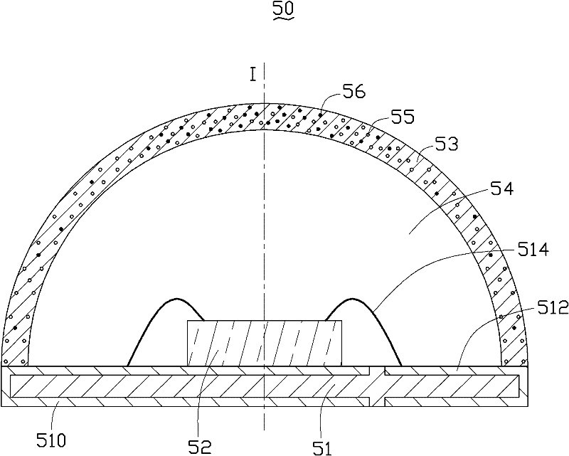
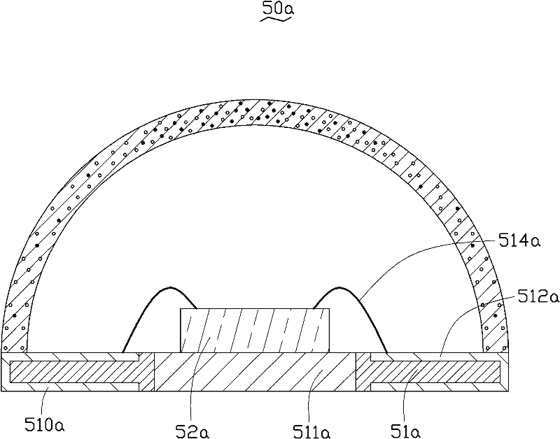
[0023] see figure 1 The LED packaging structure 50 provided in the first embodiment of the present invention includes a substrate 51, a LED chip 52 mounted on the substrate 51, a package body 53 sealed above the LED chip 52, and a package body adsorbed on the package. The light scattering structure on the body 53. Phosphor powder 55 is distributed inside the package body 53 . The light scattering intensity of the light scattering structure increases and decreases in the same direction as the intensity of light irradiated by the light emitting diode chip 52 on each area of ​​the package body 53 .

[0024] Described substrate 51 can adopt aluminum oxide (Al 2 o 3 ), silicon (Si), silicon carbide (SiC), ceramic (ceramic), polymer (polymer) or insulating quartz and other materials. The substrate 51 includes a circuit structure electrically connected to the LED chip 52 . The circuit structure includes a first electrode 510 and a second electrode 512 . The LED chip 52 is dispo...


PUM


Abstract

The invention discloses a package structure for a light-emitting diode. The package structure comprises a substrate, a light-emitting diode chip attached to the substrate, and a package body comprising fluorescent powder, wherein the package body has a light scattering structure; the light scattering intensity of the light scattering structure and the light intensity in each region of the package body are increased or decreased homodromously; and the density of the fluorescent powder and the light intensity in each region of the package body are increased or decreased homodromously. Therefore, the package structure for the light-emitting diode has the light scattering structure; under the light scattering action of the light scattering structure, the light transmission brightness of a central point of the package structure for the light-emitting diode and the light transmission brightness around the package structure for the light-emitting diode are basically the same, and the emergent light of the package structure for the light-emitting diode tends to be uniform; moreover, the density of the fluorescent powder is increased or decreased homodromously according to the light intensity, so that the mixed light of the package structure for the light-emitting diode tends to be uniform.

Description

technical field [0001] The invention relates to a light emitting diode, in particular to a packaging structure of a light emitting diode. Background technique [0002] Currently, Light Emitting Diodes (LEDs) are gradually replacing Cold Cathode Fluorescent Lamps (CCFLs) as light-emitting elements of lighting devices due to their good light quality (that is, the output spectrum of the light source) and high luminous efficiency. [0003] The existing LED packaging structure includes an LED chip and a packaging body that directly encapsulates the LED chip by dispensing. The packaging body is roughly hemispherical, and phosphor powder is evenly distributed therein. Phosphor powder is distributed directly around the LED chip. When the packaging structure of the light emitting diode is working, its temperature usually reaches 70-80 degrees. Such a high temperature will easily reduce the efficiency of the phosphor, resulting in a decrease in the light extraction efficiency and uni...

Claims


Application Information

Patent Timeline
Patent Type & Authority Applications(China)
IPC IPC(8): H01L33/48H01L33/58H01L33/50
CPCH01L33/508H01L33/507H01L2933/0091H01L2224/48091H01L2924/00014
Inventor 廖启维曾文良林志勇谢明村叶进连
Owner ZHANJING TECH SHENZHEN
Why Eureka
Try Eureka