Die peeling device with safety push-up pin

A technology for stripping devices and chips, which is applied in the manufacture of electrical components, circuits, semiconductors/solid-state devices, etc. It can solve the problems of mass production loss, reliability and productivity decline, and product productivity reduction in the IC packaging industry, and reduce needle replacement. Auxiliary process time, prevent splinters, easy to observe the effect

Active Publication Date: 2011-11-23
HUAZHONG UNIV OF SCI & TECH
View PDF5 Cites 4 Cited by
  • Summary
  • Abstract
  • Description
  • Claims
  • Application Information

AI Technical Summary

Problems solved by technology

Under the existing peeling and picking devices, thin chips with a thickness of less than 100 μm often crack or be damaged, causing large losses in the mass production of the IC packaging industry
[0003] The patent document CN 101707181A reduces the impact on the semiconductor

Method used


Image

  • Die peeling device with safety push-up pin
  • Die peeling device with safety push-up pin
  • Die peeling device with safety push-up pin

Examples


Embodiment Construction

[0047] The present invention will be further described below in conjunction with the accompanying drawings and specific embodiments.

[0048] The invention is applied to the peeling off of the chip and the sticky film in the process of IC packaging such as Flip Chip upside-down packaging, and the device includes a sleeve, a safety thimble and an adjustment mechanism.

[0049] The die-bonding film is placed on one end surface of the sleeve and fixed by vacuum adsorption, and the chips to be peeled off are adhered to the die-bonding film.

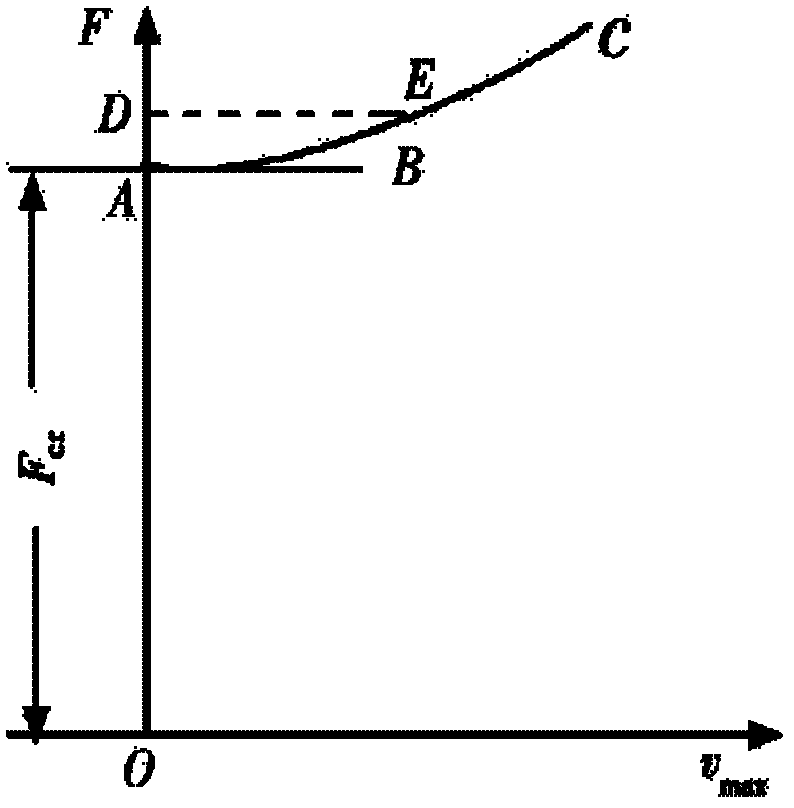
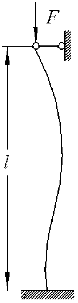
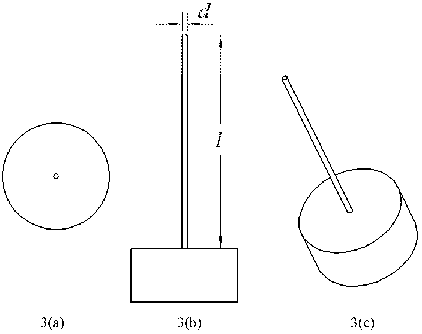
[0050] Described safety thimble, embodiment such as attached image 3 As shown, it is set in the sleeve and is used to lift the chip under the drive of the driving device to peel off the die-bonding film. The value of the force is between the chip peeling force and the chip damage force.

[0051] (1) The lower end is fixed on the thimble seat, and the upper end is against the thimble of the adhesive crystal film. It can be regarded as a sle...


PUM


Abstract

The invention discloses a die peeling device with a safety push-up pin, which can be applied to peeling a die from a bond pad in the FlipChip IC (integrated circuit) package process. The bond pad is arranged on one end surface of a sleeve, and the die to be peeled is bonded on the bond pad. The device comprises a push-up pin which is arranged inside the sleeve and used for being driven by a driving device to push up the die apart from the bond pad; and a regulating mechanism which is arranged inside the sleeve and used for holding the push-up pin and regulating the effective stress length of the push-up pin to control the Euler critical load of the push-up pin. The device is characterized in that the push-up pin is a safety push-up pin which can protect the semiconductor die from being damaged and has a preset bending feature, namely, the push-up pin bends when reaching a preset rated push-up force; and the value of the preset rated push-up force is between a die peeling force and a die damage force. The die peeling device disclosed by the invention is compatible to the conventional die peeling and pickup processes and has the characteristics of safety, high efficiency and high peeling reliability.

Description

technical field [0001] The invention relates to the technical field of packaging of semiconductor chips, in particular to a chip peeling device suitable for lifting an ultra-thin (<100 μm) semiconductor chip from a die-bonding film in a chip assembly process suitable for IC packaging technologies such as flip-chip bonding. Background technique [0002] The rapid development of various consumer electronics products and wireless communication equipment has promoted the demand for high-performance IC devices. Mobile phones, digital cameras and other wireless devices require maximum integration of functions in the smallest form factor and low-cost packages. IC packaging development Reflecting the trend of ultra-thinning, small appearance and high functional integration, in the packaging process of the device, as the chip becomes thinner, it is easy to cause cracking problems during peeling and picking. The bending stiffness of the chip is proportional to the cube of the thick...

Claims


Application Information

Patent Timeline
IPC IPC(8): H01L21/00H01L21/68H01L21/683
Inventor 黄永安尹周平彭波刘洵
Owner HUAZHONG UNIV OF SCI & TECH
Why Eureka
Try Eureka