Primary inductance correction circuit applied to flyback switching power supply

A primary inductance, correction circuit technology, applied in the direction of conversion equipment without intermediate conversion to AC, can solve the problems of reduced system design accuracy, limited integrated circuit development, lack of correction and compensation functions, etc., to achieve fast response speed and simple structure , The effect of shielding the interference of the front stage

Inactive Publication Date: 2011-11-23
XIDIAN UNIV
View PDF5 Cites 12 Cited by
  • Summary
  • Abstract
  • Description
  • Claims
  • Application Information

AI Technical Summary

Problems solved by technology

Due to the lack of corresponding correction and compensation functions in traditional integrated circuits, the influence of the deviation generated by the primary inductance on the output power cannot be avoided, resulting in a decrease in the accuracy of system design and limiting the development of integrated circuits

Method used


Image

  • Primary inductance correction circuit applied to flyback switching power supply
  • Primary inductance correction circuit applied to flyback switching power supply
  • Primary inductance correction circuit applied to flyback switching power supply

Examples


Embodiment Construction

[0037] The present invention will be described in further detail below with reference to the accompanying drawings.

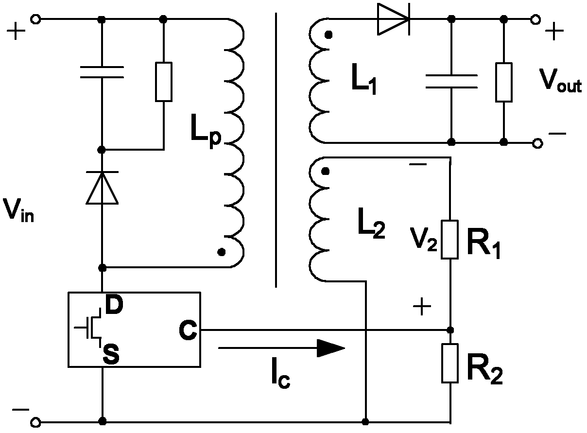
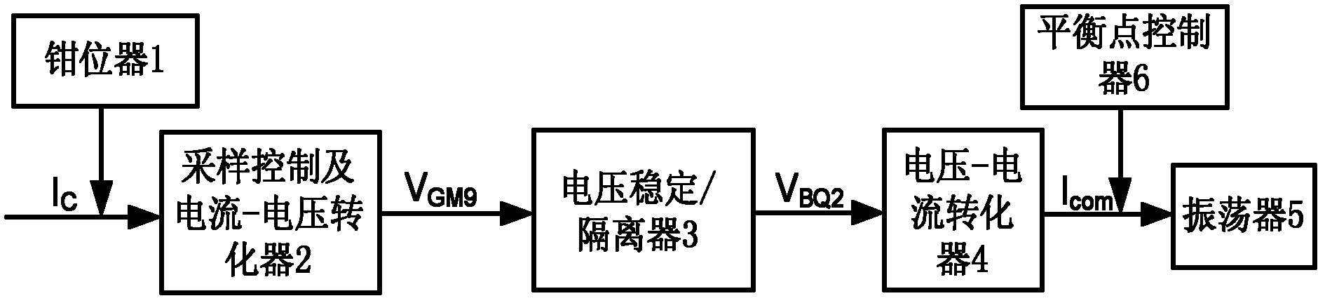
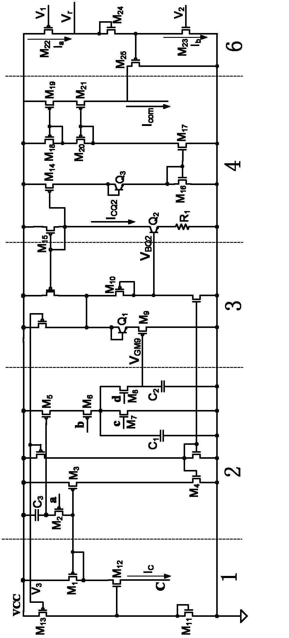
[0038] refer to figure 2 , The main modules of the present invention include: a clamper 1, a sampling circuit and a current-voltage converter 2, a voltage stabilizer / isolator 3, a voltage-current converter 4, an oscillator 5 and a balance point controller 6. Among them, the current sampling and current-voltage converter 2, the voltage stabilizer / isolator 3, the voltage-current converter 4 and the oscillator 5 are cascaded in sequence, and the clamper 1 is connected to the input of the current sampling and current-voltage converter 2 The terminals are connected, and the balance point controller is connected to the output terminal of the voltage-to-current converter 4. During the turn-on time of the power MOSFET, the clamper 1 makes the potential of the control terminal C zero, and mirrors the current flowing out of the control terminal C into the sampling curr...


PUM


Abstract

The invention discloses a primary inductance correction circuit applied to a flyback switching power supply. The primary inductance correction circuit mainly solves the problem that the primary magnetic inductance of a conventional transformer is deviated to influence output power. The primary inductance correction circuit comprises a clamper, a sampling control and current-voltage converter, a voltage stabilizer/isolator, a voltage-current converter, an equilibrium point controller and an oscillator. In the power tube conduction time of the flyback switching power supply, the sampling and current-voltage converter samples current flowing out of a control end, performs I-V conversion, voltage stabilization/isolation and V-I conversion on discontinuously sampled current, and outputs offset current. The clamper clamps the voltage at the control end to zero. The equilibrium point controller makes the offset current be zero when a primary magnetic inductance value is normal. The offset current is injected into the oscillator to change the frequency of the oscillator and further change switching frequency to correct an output power change caused by inductance tolerance. The primary inductance correction circuit has a simple structure, low power consumption and stable and accurate offset current.

Description

technical field [0001] The invention belongs to the technical field of electronic circuits, and relates to an analog integrated circuit, in particular to a primary inductance correction circuit, which can be used in a flyback switching power supply transformer in the design of a switching power supply. Background technique [0002] In the field of switching power supplies, flyback converters are especially suitable for low-power switching power supplies and various power adapters due to their simplicity, high efficiency, and low cost. However, there are many difficulties in the design process of flyback converters. Among them, due to the influence of the manufacturing process and design defects, the primary excitation inductance will have a certain range of deviation from the ideal value, which will greatly reduce the performance of the entire switching power supply and affect the working state of the chip. [0003] figure 1 It is a typical flyback switching power supply ci...

Claims


Application Information

Patent Timeline
Patent Type & Authority Applications(China)
IPC IPC(8): H02M3/07
Inventor 史凌峰来新泉才智叶强何惠森
Owner XIDIAN UNIV
Why Eureka
Try Eureka