Electrode structure and manufacturing method thereof

A technology of electrode structure and manufacturing method, applied in the direction of electrical digital data processing, instrument, data processing input/output process, etc., can solve the problem of increased contact resistance value, incomplete contact, and poor step coverage of transparent electrode layer 108 And other issues

Active Publication Date: 2011-12-07
INNOCOM TECH SHENZHEN +1
View PDF3 Cites 9 Cited by
  • Summary
  • Abstract
  • Description
  • Claims
  • Application Information

AI Technical Summary

Problems solved by technology

[0003] However in figure 1 In the vicinity of the step edge (stepedge) at both ends of the dielectric layer 106 and the metal wire 104, because the step coverage of the transparent electrode layer 108 is not good, that is, the dielectric layer 106 and the metal wire 104 The height drop makes the covering thickness of the transparent electrode layer 108 uneven, and it is easy to generate defects (defect) 105 at both ends of the metal wire 104, so that the electrical contact between the transparent electrode layer 108 and the metal wire 104 is poor. or a disconnected state, affecting the signal transmission between the left electrode 108a and the right electrode 108b, such as figure 1 As shown, a defect 105 occurs between the left end of the metal wire 104 and the left electrode 108a, forming an open loop state; the contact between the right end of the metal wire 104 and the transparent electrode layer 108 is incomplete, resulting in the transparent electrode layer The contact resistance between 108 and the metal wire 104 increases
[0004] In addition, when the area of ​​the wire not covered by the dielectric layer 106 at both ends of the metal wire 104 is too small, that is, the length L is too small, it will cause the transparent electrode layer 108 to cover the metal wire 104 poorly, which will easily cause the transparent electrode layer 108 and the metal wire 104 are disconnected, and signals cannot be transmitted between the left electrode 108a and the right electrode 108b
However, when the area at both ends of the metal wire 104 not covered by the dielectric layer 106 increases (that is, the length L is increased), metal bright spots will be formed on the capacitive touch panel, so that the appearance quality of the touch panel will be affected.

Method used


Image

  • Electrode structure and manufacturing method thereof
  • Electrode structure and manufacturing method thereof
  • Electrode structure and manufacturing method thereof

Examples


Embodiment Construction

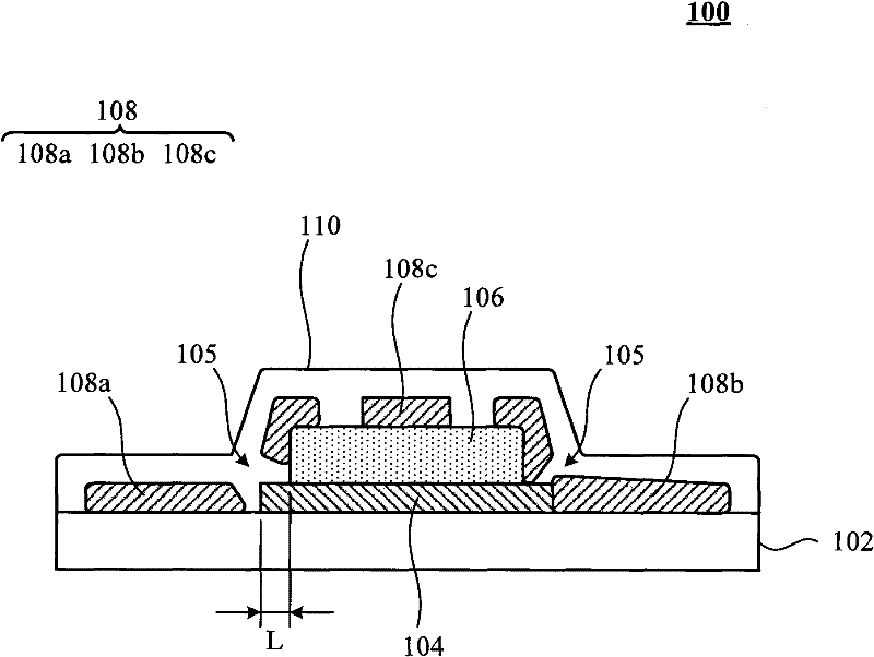
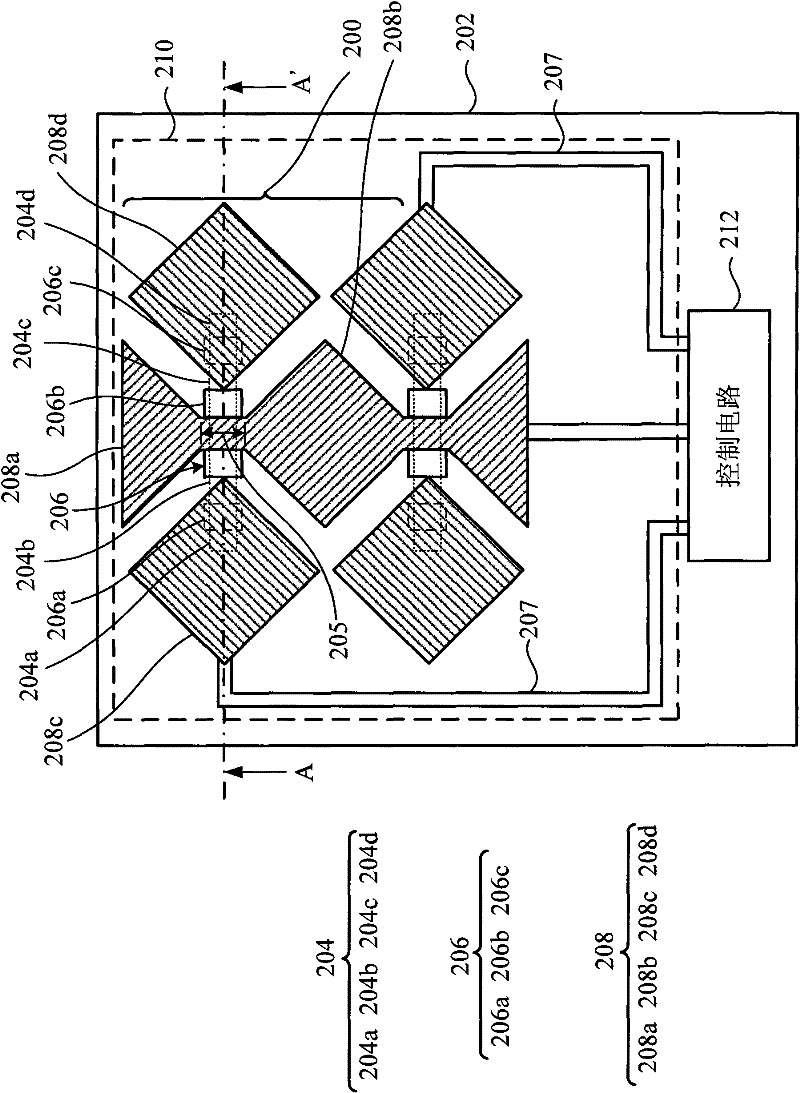
[0022] reference figure 2 , Which shows a schematic diagram of the wiring of the electrode structure in an embodiment of the present invention. The electrode structure 200 (such as Figure 3F (Shown) is suitable for capacitive touch panels. The electrode structure 200 mainly includes a substrate 202, an electrode bridge structure 204, a dielectric layer 206, a conductive pattern 208, and a passivation layer. 210. The electrode structure 200 is connected to a control circuit 212 through an electrode circuit 207. The control circuit 212 is used to process the sensing signal from the electrode structure 200. The electrode circuit 207 and the conductive pattern 208 are located in different areas on the substrate 202 . It should be noted that the above and the lower two electrode structures 200 are taken as examples here, but the present invention is also applicable to more than two electrode structures 200 to form a matrix electrode structure.

[0023] The electrode bridging struc...


PUM


Abstract

The invention provides an electrode structure and a manufacturing method thereof, including a base material, an electrode bridge structure, a dielectric layer and a conductive pattern. The dielectric layer is formed on the electrode bridge structure and the substrate and has a plurality of insulating block patterns, each of the insulating block patterns covers a part of the electrode bridge structure to form a plurality of exposed bridge patterns, each of which The insulating block patterns and each of the bridge patterns are alternately arranged in sequence along a predetermined direction. The conductive pattern has a first electrode, a second electrode, a third electrode and a fourth electrode, the first electrode is electrically connected to the second electrode, the third electrode and the fourth electrode cover the electrode bridge structure Some bridging patterns are used to reduce the contact resistance value of the electrode bridging structure with respect to the third electrode and the fourth electrode.

Description

【Technical Field】 [0001] The present invention relates to an electrode structure and a manufacturing method thereof, in particular to an electrode structure with a multi-block insulating layer suitable for a capacitive touch panel and a manufacturing method thereof. 【Background technique】 [0002] reference figure 1 , Which shows a schematic diagram of an electrode structure 100 of a capacitive touch panel in the prior art. The electrode structure 100 includes a substrate 102, a metal wire 104, a dielectric layer 106, a transparent electrode layer 108, and a passivation layer 110. The above is the use of physical vapor deposition (PVD) and lithography technology to sequentially form the metal wire 104, the dielectric layer 106, and the transparent electrode layer 108, wherein the transparent electrode layer 108 has a left The side electrode 108a, the right electrode 108b and the wire 108c, and both ends of the metal wire 104 are in electrical contact with the left electrode 108a...

Claims


Application Information

Patent Timeline
Patent Type & Authority Applications(China)
IPC IPC(8): G06F3/044
Inventor 陈文龙卢文龙曾榆钧
Owner INNOCOM TECH SHENZHEN
Why Eureka
Try Eureka