Semiconductor device and manufacturing method thereof

A manufacturing method and semiconductor technology, applied in semiconductor/solid-state device manufacturing, semiconductor devices, semiconductor/solid-state device components, etc., can solve problems such as bubble generation, stress migration failure, low dielectric constant, etc., to improve quality, reduce Contact resistance value, the effect of improving electrical function

Active Publication Date: 2006-01-25
TAIWAN SEMICON MFG CO LTD
View PDF0 Cites 2 Cited by
  • Summary
  • Abstract
  • Description
  • Claims
  • Application Information

AI Technical Summary

Problems solved by technology

[0005] By adding SiF 4 flow rate, more fluorine will be mixed into the FSG dielectric film, and the higher the fluorine concentration, the smaller the k value, however, up to about 6% of fluorine can be mixed into the FSG dielectric film (that is, bonded to Si junction), because higher concentrations will cause fluorine to escape during reactive ion etching (RIE). The fluorine escape from the FSG oxide can cause problems in copper interconnect layer systems, such as fluorine, which tends to attack copper interconnects. A connected tantalum-based liner (Ta-based liner), which produces volatile TaF 2 , and lead to the loss of adhesion between the low dielectric constant (low-k) dielectric film and the tantalum-based liner layer, the FSG dielectric film with a high concentration of fluorine is unstable, and it is difficult to deposit a cover layer or a metal layer Afterwards, and after passivation and metallization alloy treatments, bubbles are generated
[0006] There is another problem in the prior art, the FSG dielectric film has a porous characteristic higher than 5% pores (defined as 5%+, so as to be described later), which will lead to the instability of the FSG dielectric film; for example, the prior art Among them, under the conditions of using 50:1 hydrofluoric acid or 100:1 hydrofluoric acid at a temperature of about 21 to 75 degrees Celsius, the etch rate of the porous FSG dielectric film and the thermal oxide film were compared, and the result was 5%+ porous The etch rate of FSG dielectric films is about 20 times that of thermally oxidized films; for example, 5%+ porous FSG dielectric films have an etch rate of about 800 Angstroms / min for 50:1 hydrofluoric acid, while thermal Oxide films have an etch rate of about 40 Angstroms / min; use of state-of-the-art FSG dielectric films in semiconductor devices will result in metal shorts or metal bridging, and high leakage current between metals, and stress migration failures

Method used


Image

  • Semiconductor device and manufacturing method thereof
  • Semiconductor device and manufacturing method thereof
  • Semiconductor device and manufacturing method thereof

Examples


Embodiment Construction

[0036] The fabrication and use of preferred embodiments of the present invention will be discussed in detail below. In its related recognition, however, the present invention provides many inventive concepts that have applicability and that can be embodied in a wide variety of contexts. The specific embodiments discussed are merely illustrative of specific methods of making and using the invention, and do not limit the scope of the invention thereby.

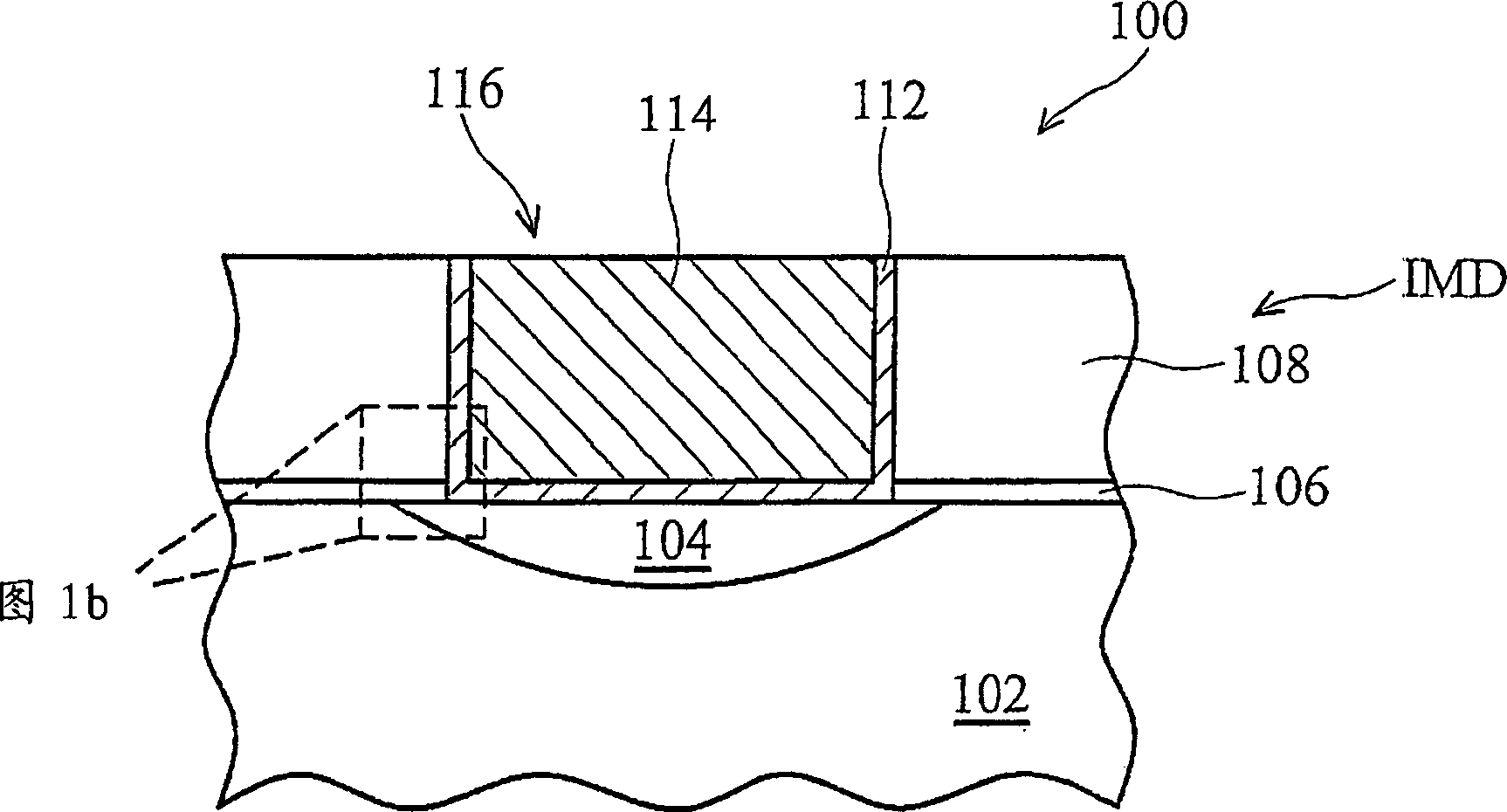
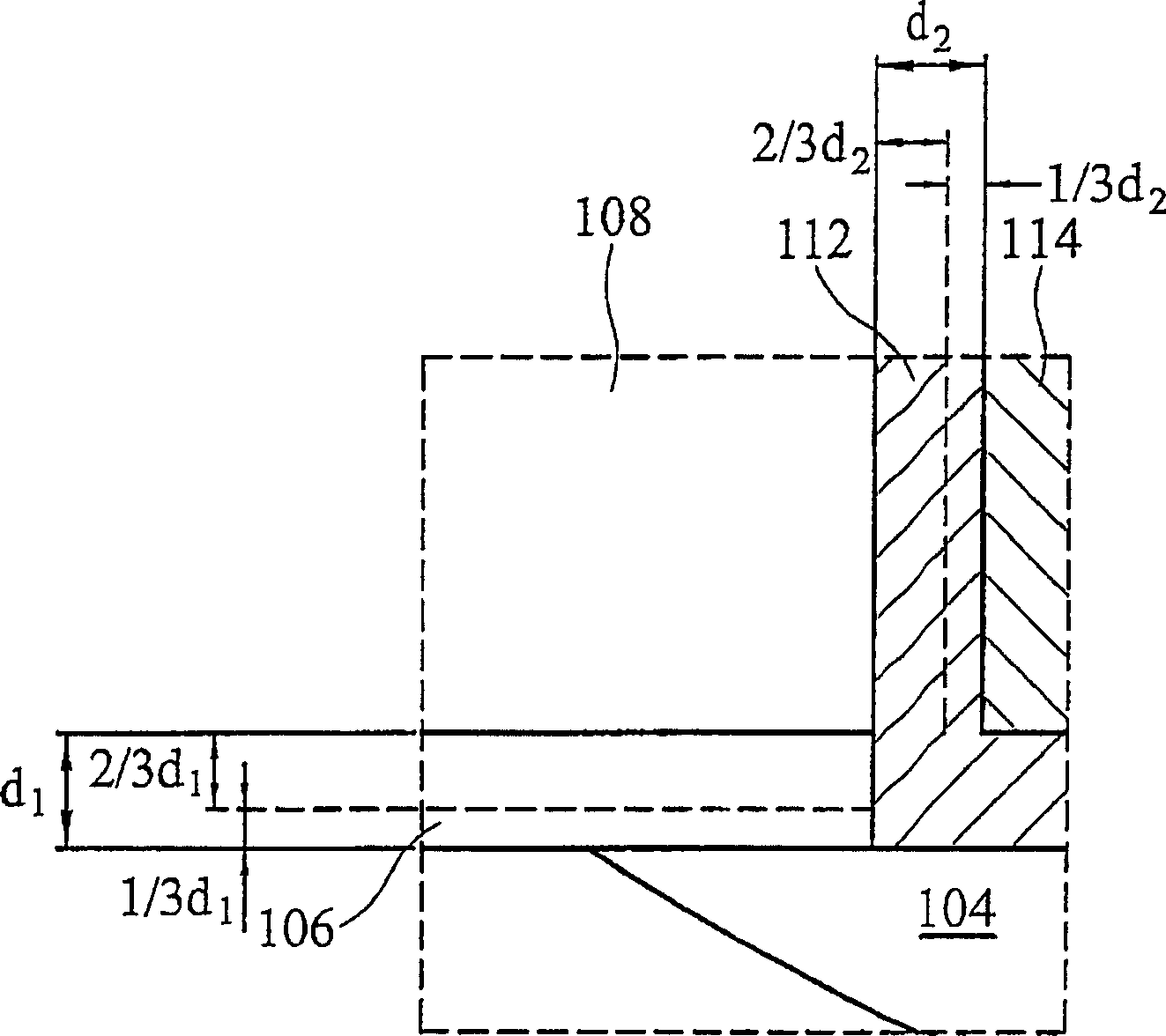
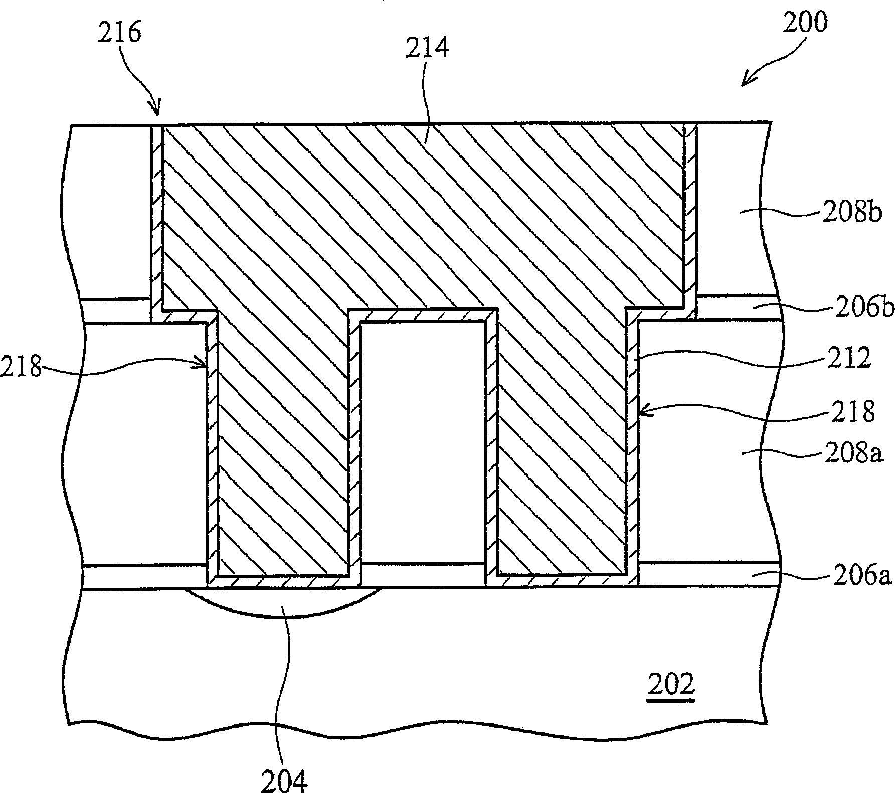
[0037] The preferred embodiment of the present invention is to form the FSG dielectric film with less free fluorine on the semiconductor substrate or device, and the embodiment of the present invention can also be applied to other technologies using dielectric materials.

[0038] A high proportion of free fluorine is found in prior art FSG dielectric films, which are not chemically bonded to silicon, for example prior art FSG dielectric films may contain approximately higher than 30% free fluorine, typically in a free state (F ...


PUM

PropertyMeasurementUnit
etch rateaaaaaaaaaa
etch rateaaaaaaaaaa
etch rateaaaaaaaaaa

Abstract

The present invention relates to a semiconductor device and a manufacturing method thereof. The manufacturing method of the semiconductor device comprises the following steps: a fluorine-containing dielectric film is formed on a substrate; the dielectric film contains about or less than 25 percent of free fluoride, about or less than 5 percent of pores and a dielectric constant of about or less than 3.8; a first diffusion blocking layer is deposited between the substrate and the dielectric film; a second diffusion blocking layer is deposited between the dielectric film and a wire. The film is formed in the following way: under the conditions when the pressure is about equal to or less than 3 Thor and the radio frequency is about between 500 watts and 5,000 watts, the gas of four fluorinated silicon and silicon methane is induced into a deposition reaction chamber; wherein, the reaction ratio between the four fluorinated silicon and the silicon methane is about equal to or less than 2.5, so as to form the fluorine-containing dielectric film. The present invention improves the quality of FSG dielectric film; and the semiconductor device that adopts the dielectric film can improve the electrical functions.

Description

technical field [0001] This invention relates to the manufacture of semiconductor devices, and more particularly to the formation of fluorine-containing dielectric films. Background technique [0002] The manufacture of semiconductor devices is to form integrated circuits by depositing and patterning one or more conductive layers, insulating layers and semiconductor layers. Some integrated circuits have multi-layer interconnection layers. The electrical layers are called inter-metal dielectrics (IMDs), and the use of multiple interconnect layers allows more chips to be produced per wafer. [0003] With the shrinking of semiconductor device size, the problems of propagation delay or resistance-capacitance delay (RCdelay) are more serious. In order to reduce delay, the semiconductor industry tends to use low dielectric constant (k) materials, which are used as insulating layers between interconnection layers To reduce the capacitance between wires. [0004] A low dielectric ...

Claims


Application Information

Patent Timeline
Patent Type & Authority Applications(China)
IPC IPC(8): H01L21/314H01L21/311C23C16/44
CPCH01L23/53295H01L21/31629H01L21/76807H01L21/02274H01L21/76802H01L21/02211H01L21/76801H01L21/02362H01L21/02131H01L21/02304H01L23/5329H01L2924/0002H01L2924/00
Inventor 吕伯雄庄学理蔡瑛修杨淑婷杨正辉冯忠铭吴斯安刘沧宇陈明德
Owner TAIWAN SEMICON MFG CO LTD
Why Eureka
Try Eureka