Die size semiconductor element package and manufacturing method thereof

A manufacturing method and semiconductor technology, applied in semiconductor/solid-state device manufacturing, semiconductor devices, semiconductor/solid-state device components, etc., can solve the problem that the packaging cost cannot be effectively reduced, and achieve material cost saving, process simplification, and quality improvement. The effect of competitiveness on rate and manufacturing cost

Inactive Publication Date: 2011-12-07
INPAQ TECH
View PDF5 Cites 5 Cited by
  • Summary
  • Abstract
  • Description
  • Claims
  • Application Information

AI Technical Summary

Problems solved by technology

[0005] The above-mentioned known semiconductor device packaging not only needs complicated processes such as die bonding, wire bonding, and molding to complete, but also needs to use a lead frame or a substrate of a

Method used


Image

  • Die size semiconductor element package and manufacturing method thereof
  • Die size semiconductor element package and manufacturing method thereof
  • Die size semiconductor element package and manufacturing method thereof

Examples


Embodiment Construction

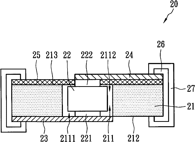
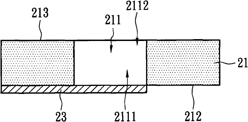
[0043] figure 2 It is a schematic cross-sectional view of a die-sized semiconductor device package according to an embodiment of the present invention. A die size semiconductor device package 20 includes a die 22 , an insulating substrate 21 having a through hole 211 , a first metal layer 23 , a second metal layer 24 and an insulating layer 25 . The first metal layer 23 is disposed on the first surface 212 of the insulating substrate 21 and the first opening 2111 of the through hole 211 . The insulating layer 25 covers the second surface 213 of the insulating substrate 21 and surrounds the second opening 2112 of the through hole 211 . The second metal 24 is disposed on the insulating layer 25 and the second opening 2112 . The die 22 is disposed in the through hole 211 and includes a first electrode 221 and a second electrode 222 . The first electrode 221 is electrically connected to the first metal layer 23 , and the second electrode 222 is electrically connected to the se...


PUM


Abstract

A chip size semiconductor element package and its manufacturing method. The chip size semiconductor element package includes a bare chip, an insulating substrate with a through hole, a first metal layer, a second metal layer and an insulating layer. The first metal layer is disposed on the first surface of the insulating substrate and the first opening of the through hole. The insulating layer covers the second surface of the insulating substrate and surrounds the second opening of the through hole. The second metal is disposed on the insulating layer and the second opening. The bare chip is arranged in the through hole and includes a first electrode and a second electrode. The first electrode is electrically connected to the first metal layer, and the second electrode is electrically connected to the second metal layer. The invention not only saves material cost, but also simplifies the process to improve the yield rate and the competitiveness of the manufacturing cost.

Description

technical field [0001] The invention relates to a semiconductor element package with a die size and a manufacturing method thereof, in particular to a semiconductor element package with a package body close to a die size and a manufacturing method thereof. Background technique [0002] In semiconductor device packaging, the bare chips are generally packaged in a plastic material or a ceramic material, which is usually called a first-level package. Packaging generally requires a carrier to support and protect the die, increase heat dissipation, and provide a system as the input or output of power and signals of the die. [0003] An important indicator of whether the packaging technology is advanced or not is that the ratio of the chip area to the packaging area is closer to 1, the better. The following are several common chip packaging technologies: (1) The initial packaging of the memory chip is a dual in-line package, that is, DIP (Dual ln-line Package), and the size of th...

Claims


Application Information

Patent Timeline
IPC IPC(8): H01L23/498H01L21/60H01L21/48
CPCH01L2224/48091H01L2224/32225H01L2224/48227H01L2224/73265
Inventor 吴亮洁王政一
Owner INPAQ TECH
Why Eureka
Try Eureka