Automatic degumming method and device for multi-wire cutting of monocrystal/ polycrystalline silicon wafer

A polysilicon wafer and multi-wire cutting technology, which is applied in semiconductor/solid-state device manufacturing, electrical components, work accessories, etc., can solve the problems of easy edge chipping and chipping on the adhesive surface, and achieve convenient application, simple device manufacturing, The effect of the method

Inactive Publication Date: 2011-12-14
沈利军
View PDF9 Cites 7 Cited by
  • Summary
  • Abstract
  • Description
  • Claims
  • Application Information

AI Technical Summary

Problems solved by technology

[0005] In order to overcome the problem that the adhesive surface is prone to chipping and chipping when degumming single crystal/polycrystalline multi-wire cut silicon wafers after deg

Method used


Image

  • Automatic degumming method and device for multi-wire cutting of monocrystal/ polycrystalline silicon wafer
  • Automatic degumming method and device for multi-wire cutting of monocrystal/ polycrystalline silicon wafer
  • Automatic degumming method and device for multi-wire cutting of monocrystal/ polycrystalline silicon wafer

Examples


Embodiment Construction

[0026] The device and method of the present invention will be further described below in conjunction with the accompanying drawings.

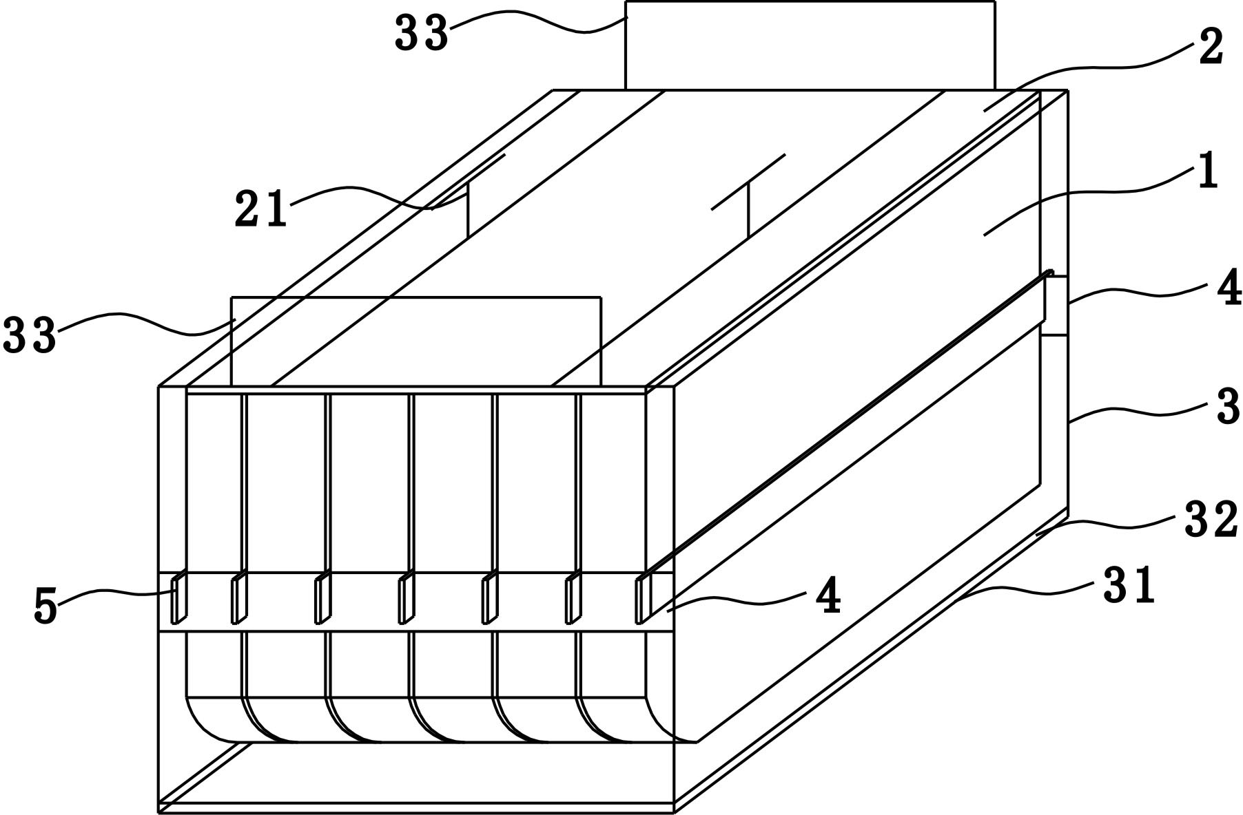
[0027] see figure 1 , this implementation case includes the workpiece (silicon wafer) 1 to be degummed on the glass strip of the connecting plate 2, and the bearing frame 3 that can accommodate the suspended workpiece (silicon wafer) 1. The bearing frame 3 includes a bottom plate 31, which is respectively arranged on the front The baffles 4 that cooperate with the workpiece (silicon wafer) 1 on the side and rear sides, the two baffles 4 on the front side and the rear side are provided with sheet-shaped positioning inserts 5 inserted in the workpiece (silicon wafer) 1 at intervals, and connecting plates 2 Suspended on the bearing frame 3, bonded to the connecting plate 2 glass strips, the bottom of the workpiece (silicon wafer) 1 to be degummed is suspended relative to the bottom plate 31, and the bottom plate 31 is laid with a buffer layer ...


PUM


Abstract

The invention discloses an automatic degumming method and an automatic degumming device for the multi-wire cutting of a monocrystal/ polycrystalline silicon wafer. The automatic degumming device comprises a workpiece (silicon wafer) which is to be degummed and is adhered to a connection plate, a bearing frame capable of accommodating and suspending the workpiece (the silicon wafer), wherein the bearing frame comprises a bottom plate and baffle plates which are arranged on the front lateral surface and the rear lateral surface and are matched with the positioning workpiece (the silicon wafer); positioning inserting strips which are inserted into the workpiece (the silicon wafer) at intervals are arranged on the two baffle plates on the front lateral surface and the rear lateral surface; the connection plate is suspended on the bearing frame; the bottom of the workpiece (the silicon wafer) which is to be degummed and is adhered to the connection plate is suspended relative to the bottom plate; and a buffer layer which drops after the workpiece (the silicon wafer) is degummed is laid on the bottom plate. By the automatic degumming method and the automatic degumming device, the influence of personal factors can be eliminated; the method is feasible and safe in operation; and the device is easy to manufacture, convenient to apply and obvious in an effect.

Description

technical field [0001] The invention relates to a degumming control technology for processing monocrystalline silicon wafers for semiconductors and monocrystalline / polycrystalline silicon wafers for solar cells in the field of multi-wire cutting, in particular to an automatic degumming method and device for multi-wire cutting of monocrystalline / polycrystalline silicon wafers. Background technique [0002] Degumming is involved in the multi-wire cutting process of monocrystalline silicon wafers for semiconductors and single crystal / polycrystalline silicon wafers for solar cells. At present, according to the different adhesives selected, there are two conventional degumming methods: [0003] One is to use cold water degumming method (such as: use American red glue), hang the cut workpiece (silicon wafer) upside down and move it together with the workpiece connecting plate into the pre-cleaning tank, and repeatedly rinse the silicon wafer with a large amount of tap water for 40...

Claims


Application Information

Patent Timeline
IPC IPC(8): B28D7/00H01L21/00H01L21/02
Inventor 汪贵发蒋建松
Owner 沈利军
Why Eureka
Try Eureka