Flexible electronic component and manufacturing method thereof

A technology of electronic components and manufacturing methods, applied in the direction of electrical components, semiconductor/solid-state device manufacturing, electric solid-state devices, etc., can solve the problem of damage to electronic components, decrease in the yield rate of flexible substrates, and the yield rate of flexible electronic components. Problems such as decline, to achieve the effect of improving the manufacturing yield rate and high manufacturing yield rate

Active Publication Date: 2011-12-14
AU OPTRONICS CORP
View PDF3 Cites 7 Cited by
  • Summary
  • Abstract
  • Description
  • Claims
  • Application Information

AI Technical Summary

Problems solved by technology

However, since the flexible substrate is closely attached to the rigid substrate through the adhesive layer, the electronic components on the flexible substrate will be damaged during the process of removing the flexible substrate from the rigid substrate. There is a possibility of damage, which will reduce the yield rate of flexible electronic components
For those with ordinary knowledge in this field, how to improve the problem of yield drop caused by the removal process of the flexible substrate is one of the problems to be solved urgently.

Method used


Image

  • Flexible electronic component and manufacturing method thereof
  • Flexible electronic component and manufacturing method thereof
  • Flexible electronic component and manufacturing method thereof

Examples


Embodiment Construction

[0034] The technical solution of the present invention will be described in detail below in conjunction with the accompanying drawings and specific embodiments to further understand the purpose, solution and effect of the present invention, but it is not intended to limit the scope of protection of the appended claims of the present invention.

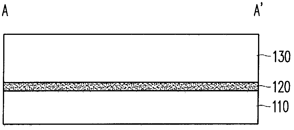
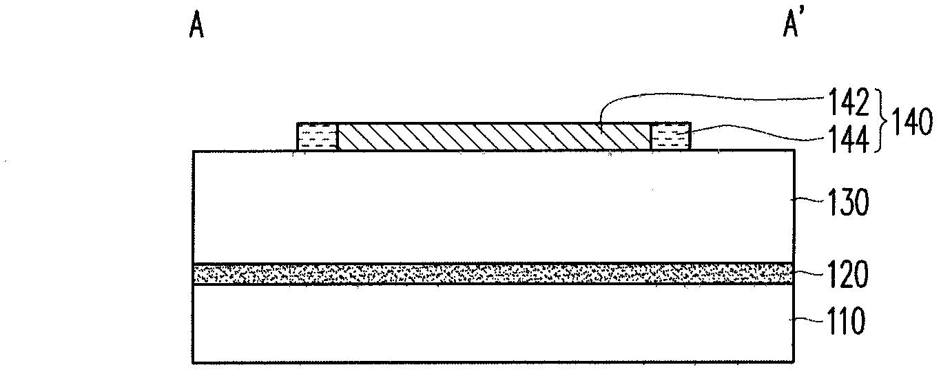
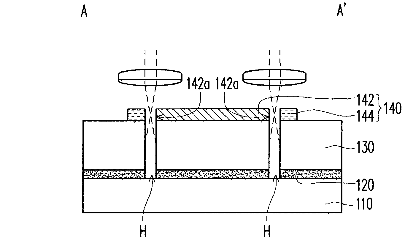
[0035] Figure 1A to Figure 1H is a schematic cross-sectional view of the manufacturing process of a flexible electronic component according to an embodiment of the present invention, and Figure 2A to Figure 2F It is a schematic top view of the manufacturing process of the flexible electronic component according to an embodiment of the present invention. In detail, Figure 1A to Figure 1D as well as Figure 1E to Figure 1F According to Figure 2A to Figure 2D The section line AA' and Figure 2E to Figure 2F is shown by the section line BB'. The following will match Figure 1A to Figure 1H as well as Figure 2A to Figure 2F , to d...


PUM


Abstract

The invention discloses a pliable electronic component and a manufacturing method thereof. The manufacturing method comprises the following steps of attaching a pliable substrate on a hard substrate through a weak-force interface layer; forming multiple array-arranged electronic components on the pliable substrate; dividing the hard substrate into multiple sub-substrate each provided with an electronic component; performing non-contact type cutting on the electronic components along at least a part of the functional part of each electronic component so as to form a first cutting channel between the functional part of each electronic component and a quasi part of the electronic component; performing contact type cutting on the pliable substrate and the weak-force interface layer along the first cutting channel so as to form a second cutting channel between the pliable substrate and the weak-force interface layer, wherein, the second cutting channel makes the sub-substrate part exposed; and removing the functional part and the pliable substrate located below the functional part from the sub-substrate. The method provided in the invention improves the manufacture good product rate of the pliable electronic component.

Description

technical field [0001] The present invention relates to an electronic component and its manufacturing method, and in particular to a flexible electronic component and its manufacturing method. Background technique [0002] Due to the characteristics of flexible electronic components such as thinness, flexibility, impact resistance, high safety and portability, flexible electronic components are bound to become the mainstream of the next generation. Generally speaking, there are two ways to fabricate flexible electronic components. One way is to directly fabricate electronic components on flexible substrates, and the other is to indirectly transfer electronic components to flexible substrates. superior. If the flexible electronic components are fabricated by directly fabricating electronic components on the flexible substrate, the flexible substrate must first be attached to the hard substrate by an adhesive layer, and then placed on the flexible substrate Make the required...

Claims


Application Information

Patent Timeline
Patent Type & Authority Applications(China)
IPC IPC(8): H01L21/02H01L21/84H01L23/14G02F1/133
Inventor 张展玮方玮嘉胡至仁
Owner AU OPTRONICS CORP
Why Eureka
Try Eureka