Imaging box chip, imaging box and identification method for imaging box

An imaging box chip and imaging box technology, applied in the direction of electrical recording technology using charge graphics, equipment using electrical recording technology using charge graphics, electrical recording technology, etc., can solve the problems of increasing production costs, lengthy production steps, and optical sensor size Small problems, to achieve the effect of improving reliability, avoiding high-precision requirements, and simplifying product structure

Active Publication Date: 2011-12-21
APEX MICROELECTRONICS CO LTD
View PDF8 Cites 24 Cited by
  • Summary
  • Abstract
  • Description
  • Claims
  • Application Information

AI Technical Summary

Problems solved by technology

[0006] However, there are certain defects in the optical structure of the above-mentioned imaging box to inform the imaging device of the remaining amount of toner: in addition to involving light-emitting components and light-receiving components, this type of method also needs to be provided with additional components on the imaging box, such as prisms, codes, etc. Wheels, reflective materials, optical inks, etc.
The cooperation between the light emitting part, the light receiving part and the additional part often makes its structure too complicated, and various detection and identification errors may occur due to the low precision of the cooperation of each part in practical applications
For example, for OEMs producing such printers, due to the very small size of the optical sensor used in conjunction with the prism, very high precision is required when setting the distance between the light emitting part and the light receiving part, which also increases production accordingly. cost; and in the process of actual use by the user, dust may intrude inside the printer, causing the light receiving part to directly receive the light emitted by the light emitting part without being reflected by the prism, which further leads to errors
For consumable manufacturers that produce compatible ink cartridges for such printers, it takes a lot of manpower and material resources to make this very high-precision prism and the corresponding optical channel. Once the prism and optical channel are not aligned with the optical sensor below, it is easy The consequences of not recognizing the machine and not being able to detect the remaining ink
For the code wheel device, since a torsion spring coupling device is used to drive the gear and the code wheel, the torsion spring will gradually age and lose its elasticity as time goes on, and the time value of the light transmission window on the code wheel is due to It is easily affected by external resistance factors such as toner and has uncertainty. The error generated by the combination of the two will seriously affect the accuracy of the imaging device to identify the imaging cartridge and monitor the remaining amount of toner
In addition, since the light received by the light-receiving part from the light-emitting part must pass through the light-transmitting window on the code wheel, manufacturers of compatible consumables must spend a lot of energy to precisely design the size and shape of the code wheel, which further adds to the Lengthy production steps and unnecessary production costs
In addition, for non-recyclable code wheel devices, it limits the development of compatible general consumables market

Method used


Image

  • Imaging box chip, imaging box and identification method for imaging box
  • Imaging box chip, imaging box and identification method for imaging box
  • Imaging box chip, imaging box and identification method for imaging box

Examples


Embodiment 1

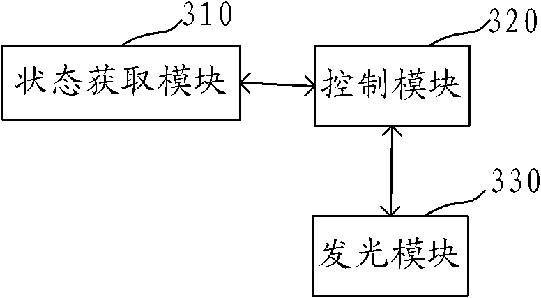
[0030] image 3 The structural diagram of the imaging cartridge chip provided in Embodiment 1 of the present invention, the imaging cartridge chip is a chip installed on the imaging cartridge, and usually records the basic information of the imaging cartridge, such as model, production date, toner type and toner amount and other data. The imaging device identifies the imaging cartridge by interacting with the imaging cartridge chip, and also updates the information in the chip by writing data into the imaging cartridge chip. The imaging cartridge chip provided in this embodiment at least includes a status acquisition module 310 and a control module 320 . Wherein, the status acquiring module 310 is used to acquire the usage status information of the imaging box; the control module 320 is connected with the status acquiring module 310, and is used to generate a light control signal corresponding to the usage status information of the imaging box according to the optical identif...

Embodiment 2

[0049] Figure 6 It is a schematic diagram of the structure of the imaging cartridge chip provided by Embodiment 2 of the present invention. This embodiment may be based on the foregoing embodiments, and specifically provides a method for obtaining the amount of toner. The dose acquisition unit 310 a in the state acquisition module 310 may include: a dose detection subunit 311 , configured to detect the toner amount from the information exchanged between the imaging cartridge chip and the imaging device, and provide it to the control module 320 .

[0050] The dose detection subunit is mainly used for reading and writing relevant data when the imaging device communicates with the imaging box, and can complete the reading and writing of information under the control of the control module. The information communicated between the imaging device and the imaging cartridge may include the remaining amount of toner, the color of the toner, the date when the imaging cartridge was firs...

Embodiment 3

[0052] Figure 7 It is a schematic structural diagram of the imaging cartridge chip provided by Embodiment 3 of the present invention. This embodiment may be based on the foregoing embodiments, and specifically provides another way of obtaining the amount of toner. The dose acquisition unit 310 a in the state acquisition module 310 may include: a consumption detection subunit 312 and a dose estimation subunit 313 . The consumption detection subunit 312 is used for detecting the consumption information from the information exchanged between the imaging cartridge chip and the imaging device. For example, the number of printed pages, etc.; the dose estimation subunit 313 is used to calculate the toner amount according to the consumption information and preset estimation rules, and provide it to the control module 320 .

[0053] The preset estimation rule may be, for example, roughly how much toner is needed to print one page, estimate the used toner according to the number of pr...


PUM


Abstract

The invention discloses an imaging box chip, an imaging box and an identification method for the imaging box. The imaging box chip comprises a state acquiring module and a control module, wherein the state acquiring module is used for acquiring the use state information of the imaging box, and the control module is used for generating an optical control signal corresponding to the use state information according to an optical identification rule of an imaging device, so as to control a light-emitting module arranged on the imaging box or the imaging box chip to emit lights towards a light-receiving part arranged on the imaging device. The imaging box chip provided by the invention can be used for controlling the light emission according to the use state information, without the light reflection and transmission of an optical additional part arranged in the imaging box, thereby avoiding the high-precision demand on optical elements and simplifying the structure of a product at the sideof the imaging box. The imaging box chip can imitate the light reflecting the use state information, thereby promoting the reliability of the imaging device for identifying the imaging box.

Description

technical field [0001] Embodiments of the present invention relate to imaging technologies, and in particular to an imaging box chip, an imaging box, and an identification method for an imaging box. Background technique [0002] As is well known, an imaging device is usually used in conjunction with an imaging cartridge, that is, the imaging device consumes toner stored in the imaging cartridge to record an image on an imaging medium. Typical applications such as printers, copiers, etc. When the imaging box is installed in the imaging device, the imaging device will judge and identify the imaging box. On the one hand, it can be determined whether the installed imaging box can match the imaging device through the installation identification information, so as to prevent the imaging device from using an illegal imaging box. On the other hand, during the imaging process, the imaging device will also timely monitor the amount of toner used or remaining in the imaging cartridge,...

Claims


Application Information

Patent Timeline
Patent Type & Authority Applications(China)
IPC IPC(8): B41J2/175G03G15/08
Inventor 刘卫臣
Owner APEX MICROELECTRONICS CO LTD
Why Eureka
Try Eureka