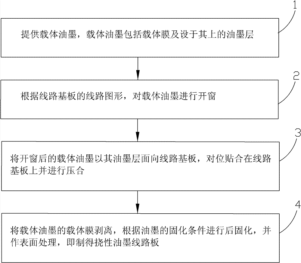
Method for manufacturing flexible printed circuit board
A manufacturing method and circuit board technology, which are applied in the secondary treatment of printed circuits, coating of non-metallic protective layers, etc., can solve the problems of high cost and labor, pollution of space environment, and low cost requirements, so as to save labor and reduce pollution. , the effect of reducing thickness
- Summary
- Abstract
- Description
- Claims
- Application Information
AI Technical Summary
Problems solved by technology
Method used
Image
Examples
Embodiment 1
[0024] Embodiment 1: The carrier ink made of green oil (model: TG1, manufactured by Lvgu Company) is used to make a flexible ink circuit board
[0025] The ink layer thickness of the carrier ink is 7 μm, and the thickness of the carrier film is 50 μm. The window is opened by punching to make a mobile phone antenna board. The normal fast pressing method can achieve good ink transfer and line protection effect. The fast pressing temperature is : 180°C, time 100s, post-curing condition 150°C / 20min; make 20 boards respectively, use carrier ink to achieve 100% yield, use silk screen printing process to produce 2.3% missing printing, partial printing and other silk screen printing defect.
Embodiment 2
[0026] Embodiment 2: Using the carrier ink made of black oil (model: TG1, manufactured by Lvgu Company) to make a flexible ink circuit board
[0027] The ink layer thickness of the carrier ink is 7 μm, and the thickness of the carrier film is 50 μm. The window is opened by punching to make a mobile phone antenna board. The normal fast pressing method can achieve good ink transfer and line protection effect. The fast pressing temperature is : 180°C, time 100s, post-curing at 150°C / 20min; make 20 boards respectively, use carrier ink to achieve 100% yield, use silk screen printing process to produce 1.5% missing printing, offset printing, etc. Silkscreen defects.
[0028] In summary, the present invention changes the traditional screen printing ink process, adopts solid carrier ink, opens a window for the carrier ink, and peels off the carrier film of the carrier ink after alignment pressing and curing, so as to achieve ink protection for the area that needs to be protected, and ...
PUM
 Abstract
Description
Claims
Application Information
 - R&D
- Intellectual Property
- Life Sciences
- Materials
- Tech Scout
- Unparalleled Data Quality
- Higher Quality Content
- 60% Fewer Hallucinations
Browse by: Latest US Patents, China's latest patents, Technical Efficacy Thesaurus, Application Domain, Technology Topic, Popular Technical Reports.
© 2025 PatSnap. All rights reserved.Legal|Privacy policy|Modern Slavery Act Transparency Statement|Sitemap|About US| Contact US: help@patsnap.com


